
 |
|
||||
BiographyChristoph Wilhelmer was born 1993 in Lienz, Austria. He received his Bachelor degree in Technical Physics from TU Wien after doing an exchange semester at the University of Bath, UK in 2017. He received his Diplom-Ingenieur degree in Technical Physics from TU Wien in 2020 where he carried out his Master Thesis in the Quantum Materials group of the Institute of Solid State Physics. In March 2020 he joined the Institute for Microelectronics where he started his PhD, focusing on defect creation mechanisms in oxides used for semiconductor applications. |
|||||
CTLs of Point Defects in SiO2 and their Dependence on the Atomic Environment
Device reliability of silicon-based electronics is strongly influenced by point defects in the oxide. In metal-oxide-semiconductor field effect transistor (MOSFET) devices, atomic defects are suspected to be responsible for reliability issues by introducing phenomena like random telegraph noise or bias temperature instability. Apart from the well-known oxygen vacancy (OV), hydrogen-related oxide defects, like the hydrogen bridge (HB) or the hydroxyl-E’ center (H-E’), have gained increased attention in recent years because of their ability to capture charges from the silicon substrate during operation. The configurations of these defects are shown in Fig. 1 (a)-(i) for different charge states. Due to the amorphous nature of SiO2, the parameters of the defects, like formation energy or charge transition level (CTL), can vary over a wide range. Every defect has unique properties as they heavily depend on their amorphous atomic environment. It is therefore challenging to investigate the defects by experiment or simulation since the analysis of defect parameters can only be done in a statistical manner.
In recent decades, density functional theory has proven to be an excellent theoretical tool to simulate real materials and to calculate the various properties of solids. By employing a hybrid functional, we can accurately analyze electronic and structural properties of point defects. In a Si/SiO2 system, the valence and the conduction band of the silicon bulk act as hole and electron reservoirs for charge trapping defects in the oxide. CTLs near the band edges of the substrate have thus the largest impact on reliability issues.
We calculated 144 defects of each kind to analyze their CTLs and the likelihood of their creation in a realistic amorphous SiO2 structure. The CTL and the formation energies of the accumulated defects are shown as a correlation plot in Fig. 2, where the color gradient denotes a characteristic atomic distance in the structure before defect creation. It can be clearly discerned that for hole and electron capturing processes the position of the CTLs relative to the band edges, and thus their contribution to device reliability effects, each have a characteristic dependence on the atomic environment near the defect for each defect type.
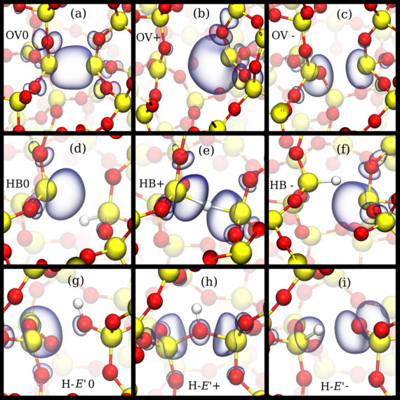
Fig. 1: Charge trapping defects in amorphous SiO2 in different charge states with their HOMO (neutral and negatively charged) and LUMO (positively charged) at an isovalue of 0.05. From top to bottom: Oxygen vacancy, hydrogen bridge and hydroxyl-E’ center. From left to right: Neutral, positively and negatively charged.
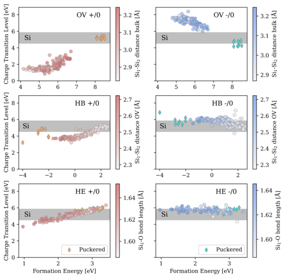
Fig. 2: Charge transition levels for hole (+/0) and electron (0/-) capture for more than 100 oxygen vacancies, hydrogen bridges and hydroxyl-E’ centers as a function of their formation energy. Band edges of the silicon substrate are shown as a gray area relative to the valence band maximum of the oxide (0 eV). The color gradient shows certain atomic distances of the precursor configurations before defect creation. OV: Distance between two silicon atoms before the oxygen atom between them is removed. HB: Distance of oxygen vacancy before a hydrogen atom is captured. H-E’: Distance between a silicon and an oxygen atom before a hydrogen atom is captured and a hydroxyl group is formed.