
 |
|
||||
BiographyAl-Moatasem El-Sayed was born in Sheffield, United Kingdom in 1988. He completed his Masters in chemistry at the University of Manchester in 2010. He went on to do his Ph.D in physics at University College, London, focussing on atomistic modeling of point defects in oxides. He then joined the Institute of Microelectronics in June 2015, his current research interests are modeling of point defects in oxides and their effect on electronic devices. |
|||||
Atomistic Modeling of Materials Used in Electronic Devices
Atomistic simulations have been integral to resolving experimental data, as well as discovering and characterizing new phenomena. High-performance computing resources combined with state-of-the-art quantum mechanical simulation codes allow one to investigate materials and their defects from first principles to a reasonably high accuracy. Our work focuses on simulating materials used in (or with potential use in) electronic devices. The following are examples of simulations we have recently made.
Point defects are a source of reliability issues in electronic devices, introducing electrostatic, as well as charge trapping, effects. Understanding their effects in a material aids in designing more reliable devices. Due to the higher charge carrier mobilities of germanium and the higher thermodynamic stability of silicon and its oxide, devices that use silicon and germanium alloys have recently become a subject of intense research. We have simulated a canonical defect, the oxygen vacancy, in mixed silicon-germanium dioxide. These simulations show that the vacancy is stable in all variations of the mixed oxide, but its behavior shows a much wider range than in either pure silicon or germanium dioxide. However, decomposing these results shows that the properties of the vacancy are mainly defined by the atoms surrounding it.
Another avenue of research being explored is defects on silicon surfaces. Despite the unfortunate nomenclature, one can exploit so-called "defects" in a rather positive way. For instance, two-state defects in silicon have led to the development of high temperature qubits, the fundamental unit of quantum information. We have recently simulated defects on silicon surfaces that could potentially be used as qubits. Combining simulations with experiment provides more concrete evidence when characterizing defects; therefore, we simulate scanning tunneling microscopy images that can be directly compared to experiment. Although it is not very trivial, the combined results offer more convincing evidence of a characterization. Fig. 1 shows an example of a dangling bond on a hydrogen passivated silicon surface, which was investigated for use as a qubit.
Finally, due to band inversion and a relatively strong spin-orbit coupling, transition metal dichalcogenides can display topologically distinct states. At the boundary between such distinct states, edges that are topologically protected are formed. These boundaries occur, for example, between a topological insulator and a vacuum, i.e. at a surface. According to topological band theory, these edge states possess highly desirable properties, such as protection from back scattering. However, recent atomistic simulations have been testing these results and assumptions, providing valuable insight into realistic topological materials. Along these lines, we have been exploring finite size effects on the topologically insulating 1T′ phase of MoS2, whose edge is shown in Fig. 2. The qualitative electronic structure showed a rich variety, which depends on the width of the topological insulator.
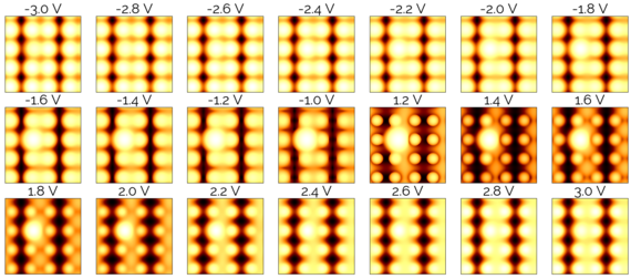
Fig. 1: Simulated scanning tunneling microscope image of a dangling bond on a hydrogen-passivated silicon (2x1) reconstructed surface.
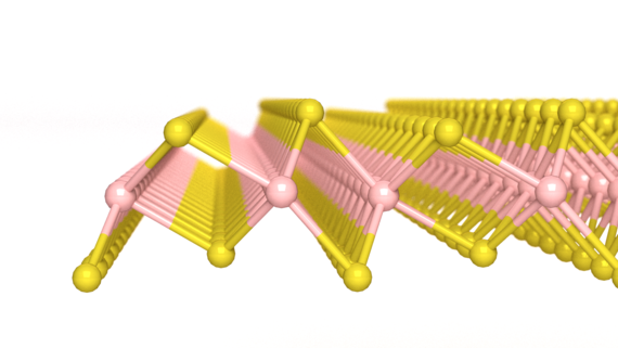
Fig. 2: The S1 edge structure of topologically insulating 1T′ MoS2.