
 |
|
||||
BiographyLado Filipovic is an Assistant Prof. (tenure-track) of Modeling and Simulation of Integrated Semiconductor Sensors at TU Wien. He obtained his Master’s degree in Applied Sciences (MASc) from Carleton University, in Ottawa, Canada, in 2009, and his doctoral degree (Dr.techn.) in Microelectronics and venia docendi (habilitation) in Semiconductor Based Integrated Sensors from the TU Wien in 2012 and 2020, respectively. He has served as a reviewer for several DFG projects, has edited a book on Miniaturized Transistors, and has reviewed for many leading journals. He is also an active member of the Technical Program Committee for outstanding IEEE sponsored conferences, such as IEEE Sensors and SISPAD. He has been a Principal Investigator in various research projects funded by, e.g., the EU FP7 and Horizon 2020 programs and the Austrian Research Promotion Agency (FFG). His primary research interest is studying the operation, stability, and reliability of novel semiconductor-based sensors using advanced process and device TCAD approaches. With his team, he is currently investigating metal oxide semiconductors and two-dimensional materials, e.g., graphene and MoS2, for the detection of environmental pollutants and biomarkers from exhaled breath. |
|||||
Application of 2D Semiconductors in Conductometric Sensors
A broad variety of two-dimensional (2D) semiconductors are currently being investigated for many potential application fields including nanoelectronic devices (e.g., transistors and memristors) and nano-sensors (e.g., gas sensors for environmental monitoring and medical diagnostics). Graphene was the first true 2D material. It is an excellent conductor, is optically transparent, and has extraordinary mechanical strength. However, extensive research into graphene has struggled to provide a working field-effect transistor (FET) due to its lack of a band gap. Nevertheless, the lessons learned from graphene have opened the scientific flood-gates to a host of other potential 2D materials that have recently risen in prominence.
Many 2D semiconductors display a band gap and have significant potential for FET applications, specifically transition metal dichalcogenides (TMDs), such as molybdenum disulfide (MoS2), and phosphorus-based films, such as black and blue phosphorene. Given their atomically thin structures, 2D materials are extremely sensitive to defects and dopants on their surface, which have a fundamental impact on their potential applications, in particular for gas sensing. In Fig. 1 (from R. Vargas-Bernal, Sensors 19, 2019), the advantages achieved in gas sensors based on 2D nanomaterials (blue squares) are compared to those based on bulk and micro-materials (green circles). The main advantages are the increased sensitivity, smaller size, shorter response and recovery times, lower working temperature, lower power consumption, and low cost. However, they are difficult to fabricate, which makes repeatability and reproducibility a potential problem.
MoS2 is a particularly interesting TMD because it is a naturally occurring crystal with a monolayer band gap of 1.8 eV and a bulk band gap of 1.23 eV, is robust, and is relatively abundant. In MoS2, defects act as primary molecular adsorption centers. The defects mainly come in the form of vacancies, most commonly a sulfur monovacancy, which can have a detrimental impact on transistor operation while playing the principal role in molecular chemisorption for potential sensing applications. In fact, MoS2 has been shown to respond to a broad range of gases at room temperature, such as H2, O2, NO, NO2, NH3, CO, and CO2, all very important for environmental monitoring and medical diagnostics.
Inversely, having too many ambient gases impact the film's performance may limit its usability in digital transistors, where the change in conductivity should be solely controlled by the gate. A further potential source of conductive variation is through strain. Its introduction in the crystal, either through lattice mismatch with the underlying insulator or through an externally applied pressure, can further complicate the conductive picture of MoS2 films. Fig. 2 shows how the band gap changes in MoS2 (left) monolayers and (right) bulk films when strain is applied. An interesting observation is that the monolayer changes from a direct to indirect semiconductor after compressive strain is applied.
A potential concern with MoS2-based devices is the films' very low experimentally achieved carrier mobility (1 cm2V-1s-1) without the use of a high-κ dielectric gate material. The use of HfO2 dielectric was shown to increase this to 150 cm2V-1s-1, which is still less than phosphorus-based 2D materials, such as blue phosphorene, which exhibits an experimental mobility of about 103 cm2V-1s-1. Blue phosphorene, an allotrope of black phosphorene with more flatly arranged P atoms, which was first proposed in 2014, is a 2D semiconductor with an indirect fundamental band gap of about 2 eV. To understand the potential of the application of this material for gas sensing, we investigate the electronic properties of pristine and doped blue phosphorene systems together with various adsorbed gas molecules.
In Fig. 3, the top and side view of the relaxed blue phosphorene structure, with an Sb dopant atom and NO2 molecule above it, are shown. The resulting electrical and physical properties, including the adsorption energy Eads (eV), charge transfer ΔQ(e), adsorption distance d(Å), and band gap Eg(eV), are given in Table 1.
| Blue phosphorene substrate |
Eg (eV) | Eads (eV) | ΔQ (e) | d (Å) | Eg (eV) |
|---|---|---|---|---|---|
| Undoped |
1.93 | -0.48 | 0.19 | 2.43 | 0.71 |
| B doped | 1.43 | -1.05 |
1.07 | 0.99 | 0.11 |
| Al doped | 1.62 | -1.08 | 0.95 | 1.08 | 1.50 |
| Ga doped | 1.60 | -0.83 | 0.86 | 1.09 | 1.49 |
| Sb doped | 1.73 | 0.00 | 0.26 | 2.09 | 0.50 |
| Bi doped | 1.59 | -0.01 | 0.26 | 1.80 | 0.35 |
From the first principles analysis, we have observed that the Sb-doped blue phosphorene has the highest response to NO2 adsorption. The conductivity increase due to the molecule adsorbing near the Sb defect is very high, resulting in a current increase from 0.73 μA to 19.47 μA, corresponding to a potential sensor sensitivity of 88%, as shown in Fig. 3.
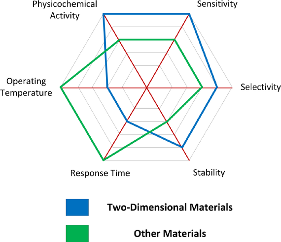
Fig. 1: The advantages achieved in gas sensors based on 2D nanomaterials (blue squares) are compared to those based on bulk and micro-materials (green circles) from R. Vargas-Bernal, Sensors 19, 2019.
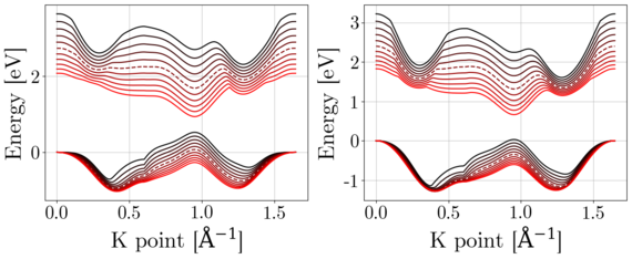
Fig. 2: Change in the band gap of a pristine MoS2 (left) nanolayer and (right) bulk films from their relaxed state (dotted line) after introducing compressive (black) and tensile (red) strain. The bands shown correspond to strain increasing from 1% to 5%.
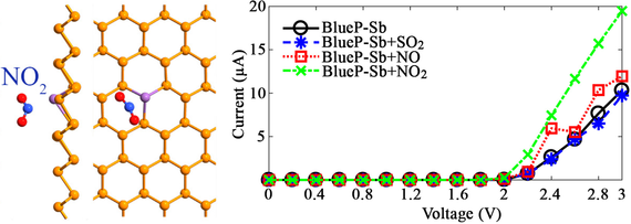
Fig. 3: (Left) Top and side view of a fully relaxed Sb-doped blue phosphorene structure with an adsorbed NO2 molecule near the dopant atom. (Right) Impact of the molecular adsorption on Sb-doped blue phosphorene on the film's conductivity.