
 |
|
||||
BiographyYury Illarionov was born in Leningrad (now Saint-Petersburg) in 1988. He studied solid state physics at the Physical Science and Technology Faculty of St. Petersburg State Polytechnical University where he received the B.Sc. and M.Sc. degrees in 2009 and 2011, respectively. From 2010 to 2012 he studied advanced material science in Grenoble Institute of Technology (France) and University of Augsburg (Germany) in frameworks of Functionalized Advanced Materials and Engineering (FAME) Erasmus Mundus program and in September 2012 received a double European M.Sc. degree. His scientific carrier has started in October 2007 in Ioffe Physical-Technical Institute (Russia) and in November 2011 he joined the PhD program there. He also visited IRCELYON (France, May-July 2011) and Singapore Institute of Manufacturing Technology (Singapore, February-July 2012) as a young guest researcher. He joined the Institute for Microelectronics in February 2013. In January 2015 he received the PhD degree in semiconductor physics from Ioffe Physical-Technical Institute and in December 2015 the Dr.techn. degree from TU Wien. Since January 2016 Dr. Yury Illarionov is a postdoc researcher working on reliability of the next-generation 2D FETs with graphene, MoS2 and phosphorene. |
|||||
Selection Criteria for Insulators in 2D Nanoelectronics
The selection of suitable insulators for 2D nanoelectronics represents an enormous challenge. This problem is of key importance, however, since scaling of 2D semiconductors towards sub-10 nm channel lengths is only possible with gate insulators scalable down to sub-1 nm equivalent oxide thicknesses (EOT).
While analyzing numerous literature reports, it becomes clear that in order to achieve competitive device performance, these insulators need to meet stringent requirements regarding: (i) low gate leakage currents; (ii) low density of interface traps; (iii) low density of border insulator traps; and (iv) high dielectric strength. Thus, we have performed a careful selection of insulators with respect to these four criteria. Previously used insulators for 2D electronic devices typically are amorphous 3D oxides known from Si technologies (SiO2, HfO2, Al2O3), but native 2D oxides (MO3, WO3 and Bi2SeO5), layered 2D crystals (hBN, mica) and ionic 3D crystals (CaF2 and other fluorides like SrF2, MgF2) have also been used or considered as promising candidates.
However, 3D oxides form poor quality interfaces with 2D semiconductors (Fig. 1a) and contain border traps which severely perturb stable device operation. The latter also applies to some native oxides, such as MO3 and WO3, which are non-stoichiometric and have a limited dielectric stability. However, other candidates, like Bi2SeO5, appear to be more promising, though an in-depth analysis of their dielectric properties is still required. HBN, on the other hand, forms excellent van der Waals interfaces with 2D semiconductors (Fig. 1b), but has mediocre dielectric properties (EG = 6eV, ε < 5) which result in excessive leakage currents for sub-1 nm EOT. The potential of other 2D insulators (e.g. mica) is currently unclear, in part due to the absence of scalable growth techniques. Thus, we suggest that for now the most promising insulators for 2D electronics are 3D ionic crystals, like CaF2 (EG=12.1 eV, ε=8.43), which form well-defined interfaces (Fig. 1c), exhibit low gate leakage currents (Fig. 1d), have a low concentration of border traps and excellent dielectric stability. Furthermore, fluorides can be epitaxially grown on large-area chips, thereby enabling fully integrated nanoelectronic devices. In summary, our comprehensive analysis suggests that 3D oxide insulators are unlikely to be suitable for integration into 2D nanoelectronic devices. Thus, an intensive search of beyond-hBN layered insulators and native oxides, as well as further development of 2D devices with epitaxial fluorides, appears promising.
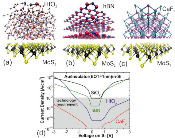
Fig. 1: Schematic structure of MoS2/HfO2 (a), MoS2/hBN (b) and MoS2/CaF2 (c) interfaces. (d) Theoretical leakage currents through these insulators for EOT = 1 nm.