
 |
|
||||
BiographyXaver Klemenschits was born in Vienna in 1994. He studied Nanoscale Physics at the University of Birmingham, England, for which he received the degree of MSc in 2017. He joined the Institute for Microelectronics in August 2017, where he is working on topography simulation using different deposition and etching models. |
|||||
Combining Process Simulation and Emulation using ViennaLS
Process technology computer aided design (TCAD) is an important component in the design technology co-optimization (DTCO) cycle used to understand the origin of process variations and to find possibilities for their mitigation. However, sophisticated physical simulations require substantial computational effort, making it often unfeasible to simulate an entire integrated circuit (IC) process flow. Nonetheless, many fabrication steps can be emulated using computationally efficient empirical models, while intricate physical simulations are only required for specific critical process steps. Therefore, in order to generate the most physical results within a reasonable time frame, we combine sophisticated physical process models with simple emulation models in the simulation framework of ViennaLS [1]. This is made possible by the geometric advection of the level set, meaning no costly conversions between surface representations are necessary, and all models can be carried out directly after one another.
Using these capabilities, we can simulate entire device structures in a matter of minutes. In order to get a process-aware description of the source and drain regions, physical models have to be employed for every process step shaping these regions. The first of these processes is fin patterning, as shown in Fig. 1, which shapes the silicon fins representing the conducting channel in the final transistor. Secondly, the spacer etch and fin recess must be modeled physically, which results in the geometry shown in Fig. 2. The last step requiring thorough physical modeling is the source and drain epitaxy, resulting in the geometry shown in Fig. 3. All prior, intermediate and later fabrication steps are emulated using empirical models. Therefore, the source and drain regions are simulated with intricate physical models to produce the most realistic geometry possible, while all other parts are emulated with empirical models to complete the electrical circuit.
[1] X. Klemenschits et al. ViennaLS. [Online]. Available: https://github.com/ViennaTools/ViennaLS
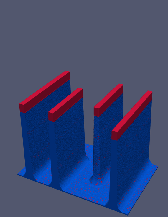
Fig. 1: Fin patterning modeled using a physical SF6 etch simulation.
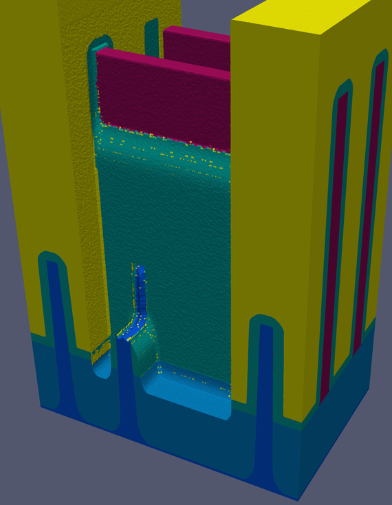
Fig. 2: Geometry after spacer etch and fin recess, freeing up the fin for the subsequent source and drain epitaxy.
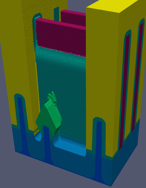
Fig. 3: Final source and drain geometry created by physical models, leading to the most realistic description possible.