
 |
|
||||
BiographyTheresia Knobloch was born in Vienna in 1992. She received her BSc degree in Technical Physics and the degree of Diplomingenieur in Microelectronics from the Technische Universität Wien in 2014 and 2016, respectively. She joined the Institute for Microelectronics in April 2016, where she is currently working on her doctoral degree. Her current research topic are novel devices based on two-dimensional materials. |
|||||
Performance Limits of Hexagonal Boron Nitride for Scaled CMOS Devices Based on 2D Materials
Complementary metal-oxide-semiconductor devices (CMOS) are a central building block of the integrated circuits all of us use daily. Progress in the field has been driven over the past 60 years by continuous scaling leading to device dimensions on the nanometer scale for state-of-the-art devices. Two-dimensional (2D) materials offer unprecedented advances in device performance at the atomic limit. While 2D semiconductors, like transition metal dichalcogenides or black phosphorus, have been well explored, suitable insulators for 2D nanoelectronics are scarce. At the moment, hexagonal boron nitride (hBN) is the most common layered insulator and is considered to be the most promising gate insulator for 2D material-based transistors.
Nevertheless, a competitive gate insulator for scaled CMOS devices needs to meet several stringent requirements. First, it needs to be scaled to ultrathin layers with an equivalent oxide thickness of less than 1 nm. Second, the insulator must sufficiently block leakage currents through these ultrathin layers, offering leakage current densities below 10-2Acm-2 for applied gate voltages of up to 0.7 V. Third, the defect density at the interface and in the insulator in the vicinity of the semiconducting channel should be as small as possible, ideally below 1010 cm-2. This is essential as interface defects increase the subthreshold swing, and border traps in the insulator degrade stability and reliability of the transistors. Fourth, the dielectric stability should be high, with an electric breakdown field exceeding 10 MVcm-1. Finally, in order to maintain high room-temperature mobility in the 2D semiconductor, remote phonon scattering must be minimized.
To meet this last criterion, hBN is ideally suited because of its comparatively small permittivity of about 5, leading to record-high mobilities measured in 2D semiconductors like graphene on hBN substrates. This motivates the idea to use hBN to screen remote phonons from an amorphous oxide, but for an effective screening, hBN interlayers of at least 3.3 nm thickness would be required (see Fig. 1). At the same time, the small permittivity of hBN also signifies that for reaching a small EOT of about 0.8 nm the physical thickness of hBN must not exceed 0.99 nm or 3 atomic layers.
On all currently available samples of hBN, the leakage currents through these thin layers exceed the acceptable low-power limit for the current densities due to high defect densities that give rise to sizable trap-assisted tunneling currents. Therefore, we aimed to answer the more fundamental question of whether in the ideal, defect-free case, future hBN samples grown with optimized processes might be able to sufficiently block tunnel currents at the scaling limit. For this purpose, we calculated the tunnel current using the Tsu-Esaki model and ab-initio DFT+NEGF calculations. See our results in Fig. 2, where the blue range of hBN tunnel currents is mostly above the low-power current limit. Therefore, excessive leakage currents through thin hBN layers make it unlikely that hBN will be suitable for use as a gate insulator in ultrascaled CMOS devices.
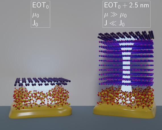
Fig. 1: Schematic drawing showing the effect of a several nanometer thick hBN interlayer at the interface of black phosphorus with silicon dioxide. Thick hBN interlayers ensure high mobilities and small leakage current densities.
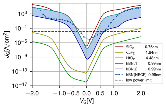
Fig. 2: Comparison of the tunnel current densities through hBN and other insulators considering the ideal case without any defects. Leakage currents through hBN (blue range) are sizable and exceed the required low-power limit for most applied gate voltages.