
 |
|
||||
BiographyChristian Schleich started his engineering career as a service engineer and technical support engineer at EVGroup, a semiconductor equipment supplier, directly after graduating from technical high school (HTL) in 2006. He studied electrical engineering at TU Wien, where he received his BSc degree in 2017 and his MSc degree in 2019. He joined the Institute for Microelectronics in February 2019 and is currently working on his PhD on the characterization and modeling of defects in SiC MOS transistors. |
|||||
Modelling of BTI for Different SiC DMOSFET Technologies
Silicon carbide (SiC) MOSFET technologies designed for power conversion applications exhibit higher drifts of the threshold voltage than their conventional Si counterparts due to an increased number of defects contributing to charge trapping. Since charge trapping at such defects, which are located close to the conducting channel, is strongly bias and temperature-dependent, the phenomenon is referred to as bias temperature instability (BTI). The impact of BTI on device behavior can be observed as a drift of the device's threshold voltage, even though constant biases are applied at each terminal of the transistor.
A detailed understanding of the transient degradation behavior and its consequences for application in power conversion circuits is currently of high research interest. This requires a physical model and defect parameters connected to properties of structures calculated using ab-initio methods. The enhanced BTI observed for SiC technologies becomes especially important for small time scales in SiC MOSFETs. A strong variation of both shape and amplitude of transient threshold voltage shifts has been reported in the literature for devices from different manufacturers and generations. Such differences arise mainly due to a variation in the defect properties (e.g. trap density NT, thermodynamic trap level ET, relaxation energy S, etc.) that determine the charge transfer reactions.
The number of model parameters makes the extraction of the trap parameters from experimental data a challenging task. In our work, we use a novel approach to semi-automatically extract these defect parameters for a two-state non-radiative multi-phonon model as implemented in our reliability simulator Comphy to compare three different SiC DMOSFET technologies. A large dataset consisting of both long-term DC MSM sequences and short-term AC stress schemes has been used to calibrate the simulation framework and extract the shown defect parameter distributions.
Our novel approach enabled us to accurately reproduce the unusual degradation of Vth in all three devices with the extracted defect bands for different bias stress and recovery conditions over many decades in time. The defect distributions show similarities with respect to ET and S for defects close to the conduction band edge, EC. However, they vary largely for defects in the lower half of the SiC bandgap and close to the valence band edge EV. The majority of our simulated defects are located within close spatial proximity to the SiC/SiO2 interface, exhibiting low values for S, and can therefore be considered interfacial defects.
These differences between the technologies are suspected to arise due to different post-oxidation annealing process conditions (e.g. temperature and annealing precursor). The calibrated simulation framework can further be used to extrapolate the degradation of the devices at digital AC bias conditions with varying high and low biases to typical device lifetimes using an analytical expression. This is of particular importance for the investigation of the operational stability of circuits made from these devices.
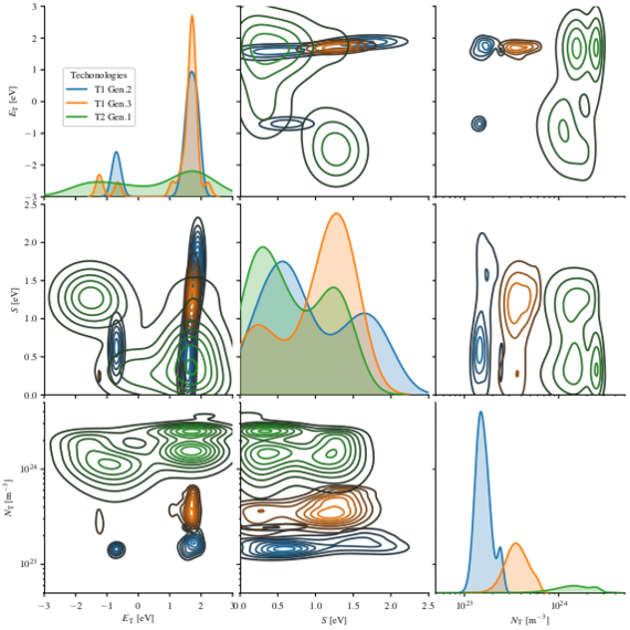
Fig. 1: Extracted defect parameters of three different SiC DMOS technologies are shown. A correlation in defect parameters for defects with ET close to EC,SiC can be observed for all three technologies.