
 |
|
||||
BiographyViktor Sverdlov received his Master of Science and PhD degrees in physics from the State University of St.Petersburg, Russia, in 1985 and 1989, respectively. From 1989 to 1999 he worked as a staff research scientist at the V.A.Fock Institute of Physics, St.Petersburg State University. During this time, he visited ICTP (Italy, 1993), the University of Geneva (Switzerland, 1993-1994), the University of Oulu (Finland,1995), the Helsinki University of Technology (Finland, 1996, 1998), the Free University of Berlin (Germany, 1997), and NORDITA (Denmark, 1998). In 1999, he became a staff research scientist at the State University of New York at Stony Brook. He joined the Institute for Microelectronics, Technische Universität Wien, in 2004. His scientific interests include device simulations, computational physics, solid-state physics, and nanoelectronics. |
|||||
Ballistic Conductance of Topological Insulator Nanoribbons
The use of new materials with advanced properties has become mandatory to meet the needs for higher electronics performance at reduced power. Topological insulators possess highly conductive topologically protected edge states that are insensitive to scattering and are therefore suitable for being employed in energy-efficient high-speed devices. The energy dispersion of such states lies in the energy gap of their bulk dispersion. The energy depends linearly on the wave vector parallel to an edge. The wave function of the edge states is strongly localized at an edge and decays exponentially along the direction away from the edge.
A two-dimensional single monolayer thin sheet of molybdenum disulphide (MoS2) in the so called 1T′ phase is an example of such a topological material. Applying an electric field orthogonal to a MoS2 sheet in the topologically insulating 1T′ phase offers a knob to manipulate the bulk spin-orbit gap. With increasing field, the gap can be reduced, closed and reopened again. After reopening, the material becomes a normal dielectric where topologically protected edge states are forbidden to exist. The ability to modulate the gap and its nature by applying an external electric field opens an alternative and complementary path to control the current flow with the gate voltage by efficiently eliminating the current carrying topologically protected states in the gap.
In order to enhance the on-current carried by the edge states, it is beneficial to have many edges by stacking several, preferably narrower nanoribbons to decrease the transistor’s footprint. In a narrow nanoribbon, however, the topologically protected edge modes whose energies lie within the energy gap of a two-dimensional ribbon can interact with each other. In order to evaluate the subband structure in a narrow MoS2 nanoribbon in the 1T′ phase, an effective k∙p Hamiltonian is employed. Due to the interaction between the edge modes from the opposite edges, a small gap in the otherwise gapless energy dispersion of the edge modes indeed opens in a narrow nanoribbon (Fig. 1). This gap rapidly increases with the perpendicular out-of-plane electric field strength (Fig. 1). This increase leads to a rapid decrease of the ballistic conductance and current with the electric field (Fig. 2), which can be used for designing molybdenum disulphide nanoribbon-based current switches.
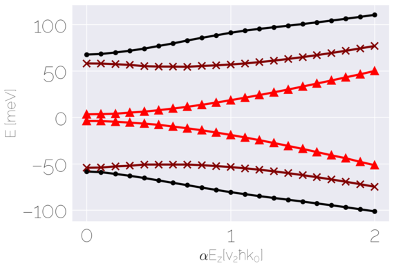
Fig. 1: Dependence of electron (hole) subband minima (maxima) on the electric field, Ez, in a narrow nanoribbon. In contrast to the bulk case, the gap never closes and keeps increasing with the electric field.
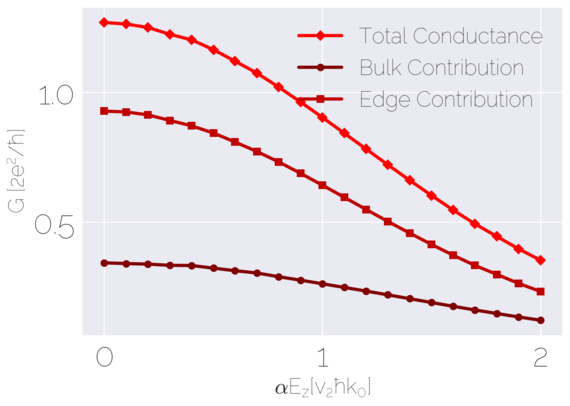
Fig. 2: Ballistic conductance (diamonds) of a 1T′-MoS2 nanoribbon, with the contributions from the edge states (squares) and the bulk-like subbands (circles).