
 |
|
||||
BiographyKonstantinos was born in Vayia, Greece, in 1994. He received the Diploma of Electrical and Computer Engineering from the University of Patras in 2018. Between 2018 and 2020, he studied at the Physics department of the National Technical University of Athens, where he received the Master's degree in Microsystems and Nanodevices. In February 2020, Konstantinos joined the Institute for Microelectronics, where he is currently working towards his doctoral degree, focusing on the characterization and modeling of charge trapping in low-noise silicon transistors. |
|||||
Distribution of Step Heights of Defects in SiON Transistors
The reliable operation of transistors is seriously affected by electron and hole traps located inside the oxide and at the oxide/semiconductor interface. Each of the single defects can capture and emit a charge, alter the device's electrostatics and modify the device's behavior. Consequently, a drift of the threshold voltage of the transistor can be measured even when constant biases are applied. This reliability issue is typically referred to as bias temperature instability (BTI). Interestingly, when devices approach the nanoscale regime, the number of defects decreases, while the impact of each single defect increases. Because of this, the charge transition events of the defects become visible as discrete steps in the drain-source current of the devices, as can be seen in the recovery trace of Fig. 1 after positive BTI stress has been applied to an SiON nMOS transistor.
A statistical description is required to describe the overall contribution of electron and hole traps to nanoscale devices because of the variability observed between nominally identical devices. Therefore, the complementary cumulative distribution function (CCDF) of step heights for each device kind can be created and analyzed (see Fig. 2). The CCDF can be explained by bi-modal exponential distributions, that allow the extraction of the average impact of a single charge and the average number of defects per device. For the employed SiON technology, a uni-modal exponential distribution of step heights of single defects has been reported in the literature. However, our results clearly show that the step heights are more likely a bi-modal exponential distribution.
To verify our extracted distributions from measurement data, we use our BTI simulator, Comphy, to simulate measured MSM-traces, which can be seen in the top part of Fig. 3. An essential ingredient in our reliability simulator is the correct replication of the impact of the steps on the overall threshold voltage, which is given by our CCDFs. This allows precise simulation of the measurement data. Finally, it has to be noted that the shape of CCDF and the area dependence of the average impact of the defects on the behavior of the device cannot be fully explained by models proposed in the literature. Thus, further investigation is required in order to resolve this issue not only for SiON, but also for SiO2 transistor technologies.

Fig. 1: Selected recovery traces showing the drift of the threshold voltage after PBTI stress, measured using scaled SiON nMOS transistors. The recovery proceeds in discrete steps in these devices. Electron (blue) and hole (red) emission events can be observed as
negative and positive discrete steps in the (ΔVth) behavior.
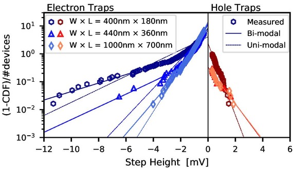
Fig. 2: Distribution of step heights measured from SiON nMOS transistors after PBTI stress for three device sets with different geometries. The majority of the observed traps are electron traps (left), but a certain number of hole traps (right) can be observed, too. The behavior of electron traps follows a bi-modal exponential distribution, while for the holes, a uni-modal exponential behavior can be observed.
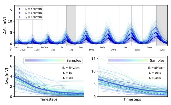
Fig. 3: In the top figure, MSM measurements (dots) at T = 100°C under three different stress conditions are shown. The lines are simulated with the BTI simulator Comphy averaged for 100 sets of sampled step heights, η, using extracted CCDFs. The regions marked grey are shown in more detail in the two bottom figures. Every light line represents a BTI simulation with a sampled set of step heights, the solid line is the average of all performed simulations.