
 |
|
||||
BiographyMichael Waltl is a senior scientist and is the director of the device characterization laboratory at the Institute for Microelectronics. He obtained the BSc degree in electrical engineering, the degree of Diplomingenieur in microelectronics, and the doctoral degree in technical sciences (summa cum laude) from TU Wien in 2009, 2011, and 2016, respectively. His scientific focus is on reliability issues in semiconductor devices and circuits, where he is investigating bias temperature instabilities in silicon devices, devices employing wideband-gap materials, and transistors built on novel 2D materials. Dr. Waltl currently leads the Christian Doppler Laboratory for Single-Defect Spectroscopy and several FFG projects. Furthermore, Dr. Waltl heads several research projects with international industrial partners imec, ams AG, Lam Research, and more. In 2018 Dr. Waltl was a visiting researcher at imec, Belgium, Europe, and at Stanford University, CA, USA. His research group at the Institute for Microelectronics counts more than 10 scientists (PhDs and PostDocs). He is also the recipient of a best paper award at IRPS 2014, a best poster award at the ICPTDC 2019, and co-recipient of the best student paper awards at the IIRW 2019, IEDM 2019, and DRC 2020. Dr. Waltl serves in the management committee of the IIRW, is a member of the technical program committee of the ESREF and ESSDERC/ESSCIRC conferences, and is a reviewer of numerous renowned Journals including IEEE TED, Microelectronics Reliability, Journal of Applied Physics, and many more. |
|||||
Analysis of Electron and Hole Trapping Components in SiON Transistors
Semiconductor transistors have become an indispensable part of everyday life and simplify our daily tasks in many ways. Almost all of our electronic gadgets are controlled by integrated semiconductor chips. To optimize the performance and the power consumption of such chips, the core components (i.e. the MOS transistors), are constantly being improved and, among other things, manufactured smaller and smaller. However, the transistors cannot be manufactured perfectly. A small number of defects remain in the oxide of the transistor or at the semiconductor/insulator interface, which influences specific device properties, such as threshold voltage. Essential effects in this context from a circuit designer's point of view are bias temperature instability (BTI) and hot-carrier degradation.
BTI is a consequence of changes in the charge state of defects, which give rise to a drift of the threshold voltage of a transistor over time and as typically analyzed after a high-stress bias has been applied at the gate of the transistor. Note that such drift can even be observed when constant biases are applied at the terminal of a device without prior stress of the device. Transistors that are only a few tens of nanometers in size are of particular interest for our research since the charge transitions of the defects can be observed as discrete steps in the drain-source current. This effect enables single-defect spectroscopy, which can precisely investigate the physical causes of the defects.
Charge trapping is primarily attributed to hole defects in pMOS transistors and electron defects in nMOS transistors. This is because, from the continuous threshold voltage drift signals measured in large transistors, it is not possible to distinguish between electron and hole traps. However, our recent single defect measurements clearly show that the superposition of both trap types determines the overall behavior. As shown in Fig. 1, we observe contributions of electron traps and hole traps in the recovery data measured on a scaled SiON nMOS transistor. The individual contributions of each trap type to the total drift of the threshold voltage are shown in Fig. 2. In nMOS transistors, the contribution of electron trapping is predominant, but hole trapping also accounts for about 20% of the threshold voltage drift. The difference between electron and hole traps is that charge transfers lead to opposite signs in their contribution to the threshold voltage. Thus, hole trapping counteracts the contributions of electron traps. The possibility to consider the partial contributions of the electron and hole traps separately also allows new insights into trap density and the influence of individual defects on the behavior of the transistors. As a consequence, single-defect spectroscopy allows for further development and significantly improves the simulation models.
Finally, we also studied the kinetics of individual electron and hole traps in more detail. The energetic trap level and local trap position can be estimated from the charge capture and emission kinetics recorded as a function of the applied voltage and temperature. Our results in Fig. 3 show that the traps lie within the active energy region of our experiments, which is an indicator of the high accuracy of our studies. As a next step, our results will support our endeavor to simulate accurate BTI-aware circuits.
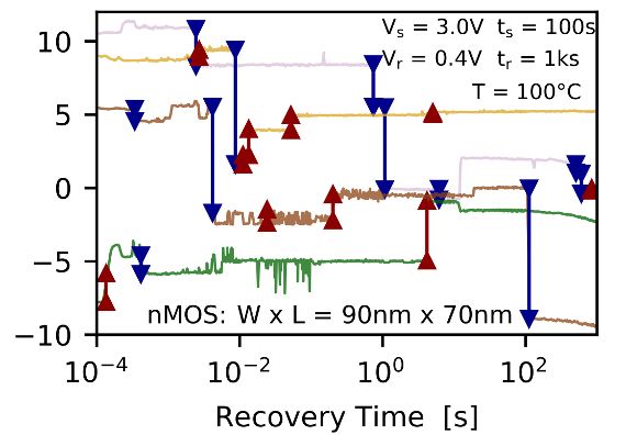
Fig. 1: Electron emission events (blue) and hole emission events (red) are visible in our single-defect spectroscopy data recorded on an SiON nMOS transistor.
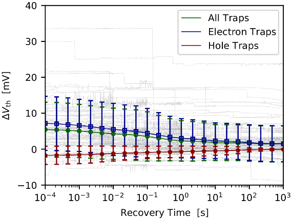
Fig. 2: The average recovery behavior of approximately 60 nMOS transistors (light grey) is shown. As can be seen, the significant contribution to the threshold voltage shift originates from the electron traps. Still, there is a sizable reduction of about 20% due to hole trapping to positive BTI.
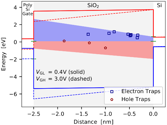
Fig. 3: The band diagram shows the trap positions and trap levels extracted for single electron and hole traps. Also shown are the active energy regions (AERs) for charge transitions between the defects and the channel (blue) and for charge transitions between the defects and the poly-gate (red). All identified traps are located in one of the AERs, confirming the accuracy of our study.