
 |
|
||||
BiographyMahdi Pourfath was born in Tehran, Iran, in 1978. He studied electrical engineering at the Sharif University of Technology, where he received the degree of Master of Science in 2002. He joined the Institute for Microelectronics in October 2003, where he received his doctoral degree in technical sciences in July 2007 and the venia docendi in microelectronics in March 2016. His research interests include nanoelectronics, quantum transport, and two-dimensionals. |
|||||
van der Waals Gap: A Hidden Factor in Transistor Scaling
As transistor dimensions continue to scale down, interface properties between semiconductors and insulators become increasingly critical for controlling electrostatics and minimizing leakage. While covalent bonding governs 3D material systems—such as the well-characterized Si–SiO2 interface—layered 2D heterostructures exhibit fundamentally different interface physics. The weak interlayer interactions between atomically thin materials lead to the formation of a van der Waals (vdW) gap, introducing a finite separation at the interface.
The absence of dangling bonds at these interfaces is often considered a key advantage of vdW gaps, contributing to reduced interface trap densities. However, the broader electrostatic and quantum mechanical consequences of the vdW gap have received comparatively little attention.
In our study, we investigated the impact of vdW gaps on gate coupling and tunneling currents across a range of insulators. Among these, hexagonal boron nitride (hBN) and strontium titanate (STO) exemplify two contrasting cases. hBN, with its atomically flat surface and low dielectric constant, forms a wide and uniform vdW gap with MoS2, which reduces leakage but weakens gate coupling. STO, on the other hand, is a high-κ oxide that supports equivalent oxide thicknesses (EOTs) below 1 nm and exhibits strong interfacial polarization with MoS2.
The figure below presents the charge density difference across hBN–MoS2 (top) and STO–MoS2 (bottom). The vdW gap distance and charge distribution within this region reduce gate leakage current but also increase the total EOT. These opposing effects highlight a trade-off: in low-κ systems, the vdW gap enables further scaling; in high-κ systems, it may impose a fundamental scaling limit.
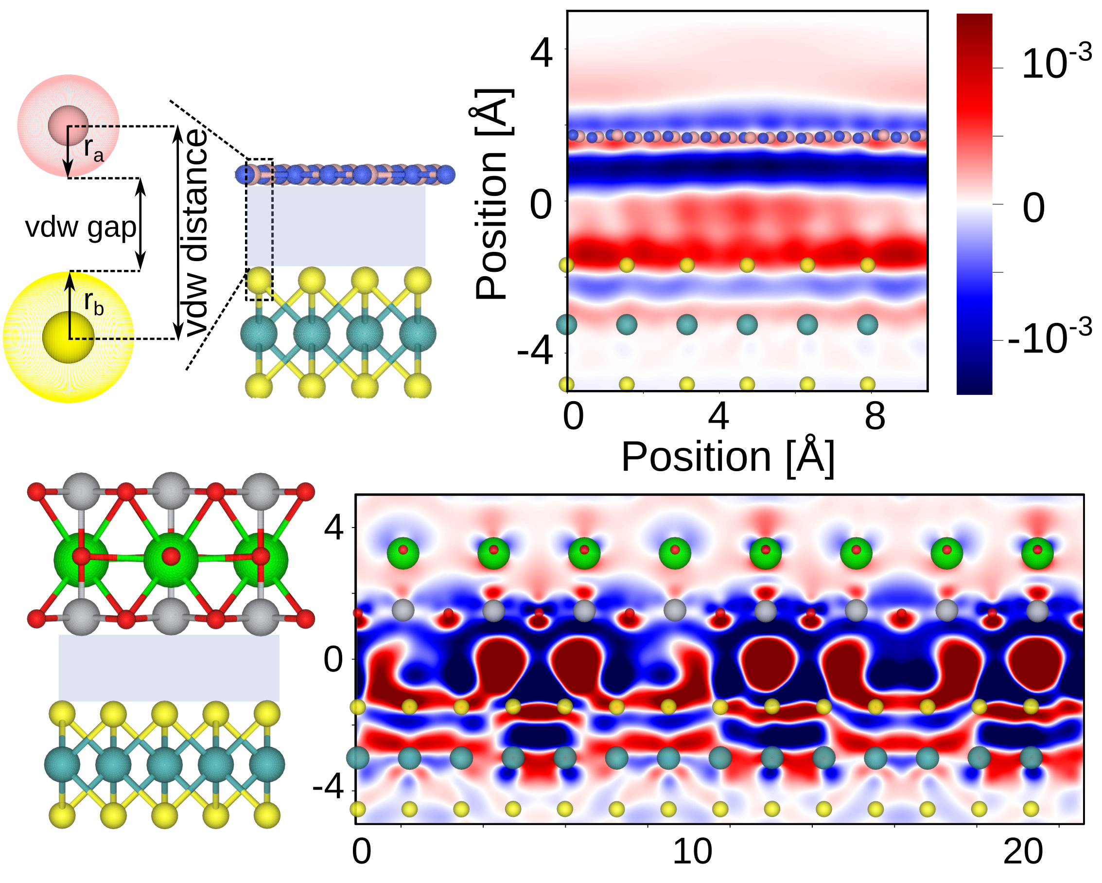
Fig. 1: Charge density difference at the interfaces of hBN–MoS2 (top) and STO–MoS2 (bottom). The contrast in gap size and interfacial charge highlights how vdW gaps influence leakage and effective gate control in 2D devices.