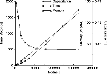
For performance investigations this basic grid has been refined in lateral and vertical direction to measure the time and memory consumption of our simulation tool in dependence of the grid points (Fig. 3). The implementation of the preconditioned CG solver in combination with the sparsely occupied stiffness matrix results in a nearly linear behavior of the time consumption. The linear dependency of the required memory is possible because of the usage of the MSCR data format for storing the quadratic stiffness matrix.
 |
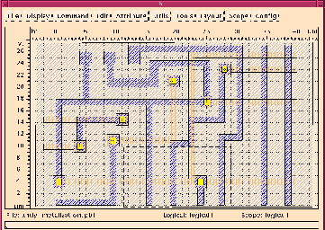
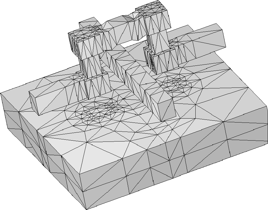
The layout of two crossing interconnects using design rules for a 0.25![]() m
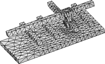
technology (Fig. 5) and non-planar deposition steps with
typical process parameters (Fig. 4) have been used to obtain
the conductor structure shown in Fig. 6 for thermal
investigations.
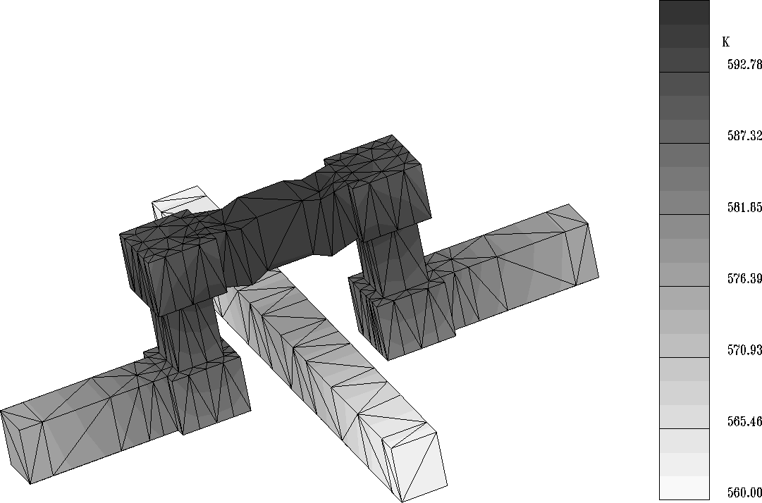
The temperature of the environment, i.e. on top and at the bottom of the
simulation domain, is assumed to be 320K.
In vertical directions we defined homogeneous Neumann boundary conditions.
Fig. 7 shows the calculated temperature distribution for a constant
current of 50mA through the Al-lines.
The temperature distribution is symmetric.
The maximum temperature of 598K occurs in the upper metal line.
This results from the larger gap between the upper metal line and the top
plane as compared to the lower line and the top of the Substrate
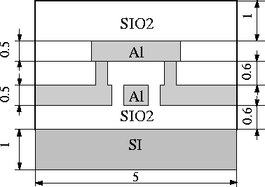
(1
m
technology (Fig. 5) and non-planar deposition steps with
typical process parameters (Fig. 4) have been used to obtain
the conductor structure shown in Fig. 6 for thermal
investigations.
The temperature of the environment, i.e. on top and at the bottom of the
simulation domain, is assumed to be 320K.
In vertical directions we defined homogeneous Neumann boundary conditions.
Fig. 7 shows the calculated temperature distribution for a constant
current of 50mA through the Al-lines.
The temperature distribution is symmetric.
The maximum temperature of 598K occurs in the upper metal line.
This results from the larger gap between the upper metal line and the top
plane as compared to the lower line and the top of the Substrate
(1![]() m vs. 0.6
m vs. 0.6![]() m cf. Fig. 4).
m cf. Fig. 4).