To model HCD understanding of the underlying physical mechanisms is naturally required, where the electric field dependence was explored first. Thus, it is not surprising that early models where based on the magnitude of the electric field in the channel (field-driven paradigm). Until today most of the models explained the influence of hot-carriers as a buildup of interface defects and charges along the semiconductor-oxide interface of MOSFETs, which are often modeled using SRH kinetics.
One of the first HCD models was the so-called Lucky-Electron model [164]. The model is based on the assumption that a single carrier (called ‘lucky electron’) is accelerated by the electric field such that it gains sufficient energy to overcome the dissociation energy barrier of a Hydrogen saturated bond at the interface. Additionally, when the lucky electron impinges on the semiconductor-oxide interface it does so without further collisions and without being scattered back into the channel. In this field-driven model the hot-carrier degradation is described as a buildup of interface states ΔNit in addition to interface states that have been active before hot-carrier stress.
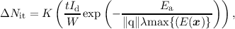
|
| (7.1) |
where K is a prefactor, t is time since the onset of stress, W is the channel width, Ea is the activation energy, λ is the electron free mean path and max{(E(x)} is the maximum electric field at the semiconductor-oxide interface. However, it has been shown (cf. Section 7.2) that HCD is not field driven and that the Lucky-Electron model fails to explain HCD in short channel devices [181]. From charge pumping experiments [182] the maximum Nit has been found not to coincide with the maximum of the electric field along the channel (cf. Figure 7.4). This, however, contradicts the prediction of the Lucky-Electron model, where maximum Nit and the peak of the electric field coincide.
While the first hot-carrier degradation models were based on the channel electric field as the driving force, it has long been realized that the phenomenon is energy- rather than field-driven [172, 176, 177]. Thus, a physics based model requires information on the energy distribution of the charge carriers. Such a model has first been proposed by the group of Hess [183, 184], improved by the group of Bravaix [162, 185] and has been constantly further developed in [174, 186], resulting in the latest carrier energy distribution based model [163], which will be presented and discussed here.
Our physics-based model, as many other models, describes the drain current and the degradation of other device parameters (e.g. Ron) as the result of a stress induced buildup of interface defects. Thus, the bond breakage mechanism needs to be addressed first. Contrary to the Lucky-Electron model the silicon-hydrogen bonds, present in every forming gas annealed device, are modeled as truncated harmonic oscillators and not by a single bond energy (cf. Figure 7.7).
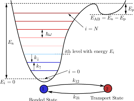
| Figure 7.7: | The truncated harmonic oscillator model of the Si-H bond used in the derivation of the HCD model. In this model, the Si-H bond is intact in state 1 (blue circle) and in the anti-bonding state 2 (red circle) it is broken. Impinging carrier can induce a vibrational mode of the bond, thereby exciting the bond. Once excited to a higher level, the bond can be more easily dissociated (i.e. the hydrogen can overcome the potential barrier separating the bonded and transport configurations) either thermally or by a carrier bombarding the interface. This is because the more the bond is vibrating, that is the higher the oscillator level that is occupied, less energy is needed to rupture the Si-H bond. |
In the truncated harmonic oscillator model of the Si-H bond, charge carriers are assumed to be able to scatter at the Si-H bond, thereby exchanging energy with the bond and scattering back into the substrate. If a sufficient amount of energy is transferred to the Si-H bond from the channel carrier, the bond is ruptured and Nit increases. This bond breakage mechanism is termed anti-Bonding (AB) mechanism and corresponds to bond rupture by a single highly energetic carrier. If the charge carrier, however, does not have enough energy to break the Si-H bond, it is assumed that this carrier at least increases the vibrational energy of the Si-H bond, thereby contributing to the multi-vibrational excitation (MVE) process. This situation corresponds to bond dissociation by a series of ‘cold’ carriers [184]. The MVE process is especially important for scaled devices, where only few charge carriers reach kinetic energies beyond the dissociation energy of the Si-H bond (≈ 1.5eV).
The truncated harmonic oscillator can be described by a set of rate equations, which read
∂tni = 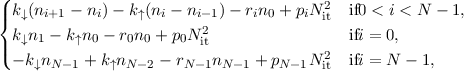 | (7.2) |
| ∂tNit | = (Nit,max - Nit)R - Nit2P, | (7.3) |
| where R | = C ∑
mN-1r
m m,P = ∑
mN-1p
m,withC = ∑
mN-1 m,P = ∑
mN-1p
m,withC = ∑
mN-1 m, m, | (7.4) |
Nit(t) = 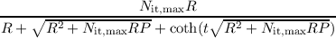 . . | (7.5) |
 and pi = 0 for all other levels, where νp ≈ 1013∕s is an attempt frequency.
The dissociation rate for the ith level with energy Ei is
and pi = 0 for all other levels, where νp ≈ 1013∕s is an attempt frequency.
The dissociation rate for the ith level with energy Ei is
ri = IAB,i + νr exp , , | (7.6) |
k↑ = IMVE + ω′exp and k↓ = IMVE + ω′ and k↓ = IMVE + ω′ | (7.7) |
IAB,i = σ0 ∫
Eth∞fn∕p(x
it,E,t)gn∕p(E)v
gn∕p(E) (E (E  =-Eth)∕Eref =-Eth)∕Eref![]](diss431x.png) 11dE, 11dE, | (7.8) |
IMVE = σ0 ∫
Eth∞fn∕p(x
it,E,t)gn∕p(E)v
gn∕p(E) (E - (E - =Eth)∕Eref =Eth)∕Eref![]](diss434x.png) dE, dE, | (7.9) |
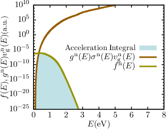
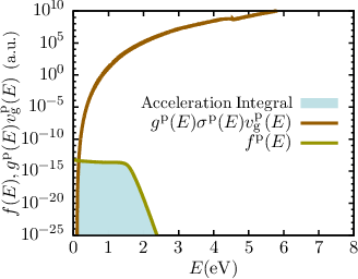
| Figure 7.8: | Exemplary distribution functions and acceleration integrals (shaded area) for electrons and holes from the middle of an artificial short channel (25nm) n-channel MOSFET simulated with ViennaSHE [65] at hot-carrier stress with phonon and impurity scattering only. Well visible is the importance of the high energy tail for the calculation of the acceleration integral. |
The defect precursors (passivated Si-H bonds) at the semiconductor-oxide interface, even in modern semiconductor devices, are not of the same atomic and energetic configuration. This is due to the amorphous nature of the employed dielectrics and lattice mismatches at the interface. Thus, the energy needed to break Si-H bonds is naturally dispersed [188], which is in our model reflected by a normal distribution of Ea. The mean value of the activation energy was chosen to be 1.5eV with a standard deviation of 0.15eV, in good agreement with experimental data [171]. The importance of the activation energy dispersion was shown in [163]. Additionally, the dipole moment d of the bond needs to be accounted for when dissociation occurs from the ith level [185]. This is done by subtracting d⋅Eox from the energy Ea - Ei needed to break the bond (cf. Equation (7.6)). To account for the dispersion of the activation energy Ea a Monte Carlo method, similar as for random discrete dopands, is used. Since any Monte Carlo method adds numeric noise to the solution another, deterministic approach can be taken: For example, assuming that the activation follows a Gaussian distribution one can sample this distribution using a sufficient number of sample points and calculate weight factors using the Gaussian distribution. Then for each sample point the model equations are being solved, where every Nit value is multiplied by the weight factor of the sample point such that the maximum Nit cannot be exceeded (normalization).