7 Hot Carrier Degradation
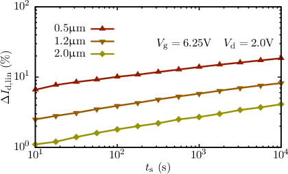
Hot-carrier degradation (HCD) is a change in the device parameters, such as drain current ΔId,
threshold voltage Vth and on-resistance Ron, in MOSFETs operating at high lateral (along
the channel) electric fields. HCD was initially only attributed to a defect buildup in the
oxide caused by hot charge carriers. However, it was found that colder charge carriers,
that are carriers with a low average energy, can also cause hot-carrier degradation [162].
Nevertheless, our latest [163] as well as older HCD models [164] include the assumption that
hot charge carriers, which have gained sufficient kinetic energy, scatter with passivated
dangling bonds at the interface, causing the bond to break. However, newer models include
the additional assumption that multiple colder carriers can also cause these bonds to be
dissociated. This rupture in turn creates Pb centers at the semiconductor-oxide interface
[165, 166], which capture and emit charge carriers, thereby distorting important device
characteristics such as e.g. drain current and threshold voltage (cf. Figure 7.1). In contrast to bias
temperature instability (BTI), however, hot-carrier degradation is best observed at high
electric fields along the channel. Whereas BTI is best observed at high gate voltages and
negligibly small lateral electric fields, such that low field conditions in the direction of charge
carrier transport are met. It is adopted that oxide defects and border traps play a crucial
role in BTI modeling, where the charge trapping kinetics are described by non-radiative
multiphonon theory [29]. In HCD modeling, however, it is assumed that Pb centers created
by hot carriers can be described by standard SRH theory and that oxide defects can be
safely neglected. Nevertheless, oxide defects were shown to be present in devices subjected
to hot-carrier stress [167]. For instance, in [168, 169] it has been demonstrated that
charging of different types of traps can lead to a change of sign in ΔId,lin. Thus, in [169]
first the ΔId,lin increases followed by a reduction in ΔId,lin at longer stress times. Such a
turned-around effect of the threshold voltage, which is attributed to the interplay of hole
trapping by bulk oxide traps and electron capture at the interface has been reported in [167].

