2.6 Quantum Mechanical Effects - Confinement
Until now purely quantum mechanical effects, such as charge carrier confinement, have not been
addressed. In MOS structures, considered in this work, carrier confinement emerges whenever
local potential wells are formed [50]. Deep potential wells cause discrete quantized energy
levels and confine the charge carriers in one or more directions. One of the most widely
recognized case of carrier confinement occurs in all MOSFETs at the semiconductor-insulator
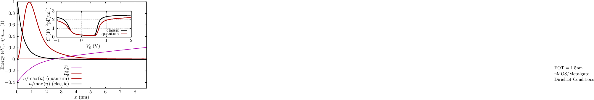
interface, whenever the MOSFET is driven into inversion as shown in Figure 2.10. In this case
the charge carriers are confined in the direction perpendicular to the interface and free
to move in the other two directions, thus forming a two dimensional electron gas [50].
When deriving the BTE in Section 2.2, the wave character of the electrons was assumed to be
negligible in favor of a classical description of the physical system. In MOS structures with thin
insulators in the range of nanometers, e.g. tox 1nm, charge carrier confinement needs to be included
in order to yield an accurate description of the device. For an accurate quantum mechanical
description of carrier confinement the Schrödinger equation
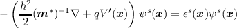 | (2.56) |
for a given confining electrostatic potential V ′(x) must be solved (self-consistently) with Equation
(2.27), where s is the sub-band index and ϵs is the energy eigenvalue. In order to solve the above
equation boundary conditions need to be set for an isolated device. It is natural to assume vanishing
electron wave functions at the boundaries of the semiconductor. If one is interested in the penetration
of the wave function into an oxide in order to calculate direct tunneling currents [52] this can be
achieved by setting a Dirichlet boundary condition at the boundaries of the oxide not interfacing with
a semiconductor, although the method itself is dependent on the oxide thickness and only justified for
thick oxides.