5.1 Composition of the Simulated
Device Geometry
In Figure
5.1 a typical scanning electron microscope (SEM) photograph of a HEMT
is shown. The epitaxial layers cap, supply, channel, and buffer are indicated
in the picture. The physical interfaces between the epitaxial layers are
considered to be abrupt. The ohmic contacts source and drain can be identified
by a rough metal/semiconductor interface which is caused by an alloying
process. In contrast to source and drain the gate Schottky contact exhibits
a smooth interface.
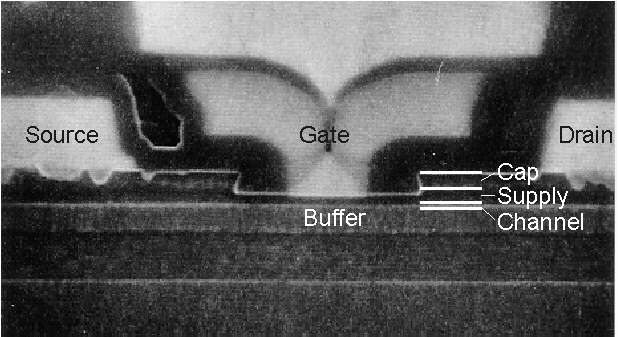
Note that at the ohmic contacts no metal penetrating through the cap layer into the supply or even into the channel layer can be observed. It is discussed that some material which behaves like a dopant in the semiconductor might diffuse into the layers or even that metal might reach the channel by spiking. An important issue which is still under discussion is the actual mechanism of current flow from the ohmic contacts into the semiconductor and through the heterojunction layers in HEMTs.
Based on the different assumptions basically three simulation models for the ohmic contacts can be developed and will be investigated in the following:
(A)
Ohmic contact only on top of the cap layers.
(B)
Ohmic contact on top of the cap layers with high doping between the contacts
and the channel.
(C)
Ohmic contact directly on the channel.
In Figure
5.2 a schematic cross section of the investigated HEMTref
is shown. The hatched areas under the ohmic contacts indicate the regions
for which the different models are used, i. e., nominal specified MBE-grown
layers, nominal layers but with doping and contact metal.

In Figure
5.3 measured transfer characteristics of HEMTref
are shown (bold line without symbols) along with three different simulations.
All three simulations are performed with the nominal layer sequence, HD
transport model in the channel and in the supply, and DD model in all other
semiconductor layers. One mechanism for electrons to cross the energy barrier
between the channel is to heat up and surmount the energy barrier which
is referred to as real space transfer (RST). This mechanism is included
in all three simulations by applying the HD model in the channel.

Using the contact model (A), i. e. ohmic contacts only on top of the cap layers, the simulation can be performed either with a thermionic emission (TE) model, which does not include tunneling, or with a thermionic field emission (TFE) model, i. e. including tunneling as described in Section 4.2.1.
The results using a TE model and contact model (A) (squared symbols in Figure 5.3) reveal very low current. Without tunneling obviously too few electrons are able to surmount the energy barrier between the channel and the supply. Even when a constant doping concentration of ND = 3.0*1018cm-3 is added in the simulation (contact model (B)) the characteristics are not improved significantly (triangle symbols in Figure 5.3). For the simulation applying a TFE interface model without additional doping (circles in Figure 5.3) the simulated and measured data agree very well.
As described before the third possible approach for the ohmic contacts of HEMTs is based on the assumption that metal from the ohmic contacts spikes through the AlGaAs supply layer facilitating an ohmic contact directly on the channel (contact model (C)). In this case most electrons would not have to cross the energy barrier between the channel and the supply but would be conducted directly from source through the channel to the drain. This is a very commonly used assumption for heterostructure devices [52, 53, 54].
Two aspects of this model will be investigated in the following. The first is the consequences of this contact model on the simulated current transport in HEMTs and the resulting characteristics. The second aspect is experimental results to gain more insight into the ohmic contacts of manufactured HEMTs.
In Figure
5.4 simulation results of the device with ohmic contacts directly on
the channel (contact model (C))
are compared with simulation results of the device with nominal layer structure
(contact model (A)).
Both simulations were performed using the TFE interface model. The threshold
voltage of the simulation with directly contacted channel was adjusted
by assuming a 10 % lower delta doping concentration than for the simulation
with contacts only on the cap. The experimental results of HEMTref
and the two simulated characteristics are very similar near VT.
But for VGS > 0.0 V the current in case of model (C)
is much higher than in case of model (A)
as well as the measured values.

More insight is gained by Figure
5.5 which shows the two simulated and the measured gm.
The magnitude of the maximum transconductance gm max and the
VGS where it is reached is among the most important DC parameters.
Both are overestimated if the channel is contacted directly. Moreover,
neither the reduction in gm for VGS > 0.0 V nor the
second local maximum in gm, which refers to the parasitic MESFET,
is reproduced. Using contact model (A)
with realistic parameters for the models the simulated and measured characteristics
coincide extremely well. The used model parameters and the way they are
obtained will be described in Section 5.3.2.

The simulation results with the contact model (A) and the measurement agree very well. Therefore this contact model seems to be more suitable though this is still not sufficient evidence. It has to be investigated whether the discrepancy of the simulation results with directly contacted channel is a consequence of an unsuitable contact model or just inadequate model parameters.
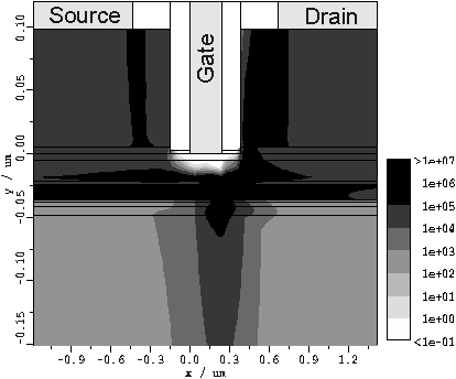
The different setups for the ohmic contacts lead to significant differences
in the simulated carrier transport properties of the HEMTs. In Figure
5.6 and Figure
5.7 the current densities for the two cases are shown both for VDS
=2.0 V and VGS = 0.5V. This corresponds to a bias point
between the two local maxima of the transconductance given in Figure
5.5. In both cases the channel can be identified by the layer with
the highest current density.
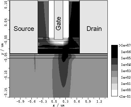
If the ohmic contacts are directly on the channel as shown in Figure 5.6 most of the electrons flow directly from source through the channel to the drain contact. Therefore the current through the channel is still governed almost linearly by the gate and real space transfer is underestimated. If the contact resistance in the simulation would be reduced to zero and the current flow over heterojunctions prevented (no tunneling) this would correspond to the intrinsic transistor.
If the contacts are only on top of the cap layers as shown in
Figure
5.7 the electrons have to cross the energy barrier between the channel
and the supply beneath the end of the gate. Moreover, for high currents
the electrons heat up and start to surmount the barrier already under the
gate. Therefore more current is conducted in the barrier layers where their
mobility is rather low and thus gm is reduced. This effect is
not only important for modeling the transfer characteristics but also to
describe short channel effects as will be discussed in Section
5.3.2.2.
The simulation study shown so far leads to the assumption that the measured device can be modeled very well with contacts only on top of the cap layer and an interface model which includes tunneling. More evidence that this contact model is a very realistic assumption is obtained by aspects obtained from experimental results.
The directly contacted channel model relies on the assumption that contact
metal spikes through the cap and the barrier layers along with doping high
enough to facilitate an ohmic contact to the channel. This mechanism either
depends on the thickness of the cap and the barrier layers through which
spiking should occur, or the spiking has to be much deeper than the thickness
variations of the layers between ohmic contact and channel.

To investigate this issue two DH-HEMTs with double recess were fabricated
which basically differ only in the thickness dS of 7
nm and 42 nm indicated in Figure
5.8. In Figure
5.9 the measured transfer characteristics of the two HEMTs are shown.
The two devices were produced in different technology runs which resulted
in a shift of VT due to slightly different recess depths.
A more positive VT, obtained for the device with dS
= 42 nm, usually leads to a higher gm max but to a lower
ID max. In addition to a more positive VT
this device has a 35 nm larger dS than the other device,
but ID max is significantly larger. If the depth of spiking
would be in the order of 120 nm (thickness of cap and supply) one would
expect a reduced ID max. Thus, if spiking is an appropriate
assumption the depth has to be much deeper than 120 nm. It is believed
that the reason for the enhanced ID max is a reduction
in crystal damage which usually occurs by etching the double recess in
the cap layer as shown in Figure
5.8.

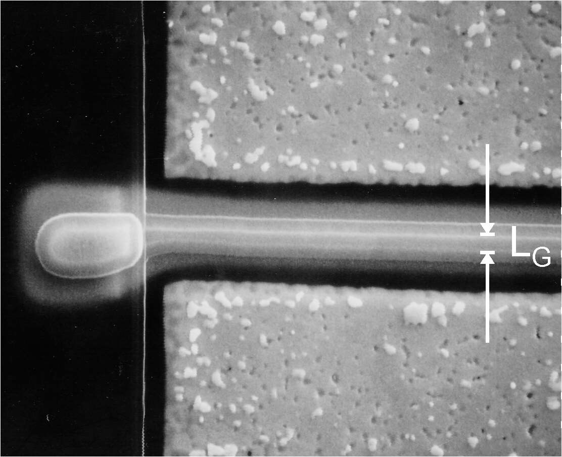
To close the chain of proof against spiking the depth of the ohmic contact
metal penetrating into the semiconductor is estimated. Figure
5.10 shows a SEM photograph of a HEMT with alloyed ohmic contacts from
the bottom. With a special preparation technique the semiconductor was
removed. The Tshaped gate finger can be clearly identified between
the ohmic source and drain metals. The light spots on the ohmic contacts
show some remaining semiconductor material. The dimensions can be estimated
by comparison to the gate length which is about 200 nm. It is evident that
the total contact area is much smoother than 200 nm. Therefore it is clear
that the HEMT cross section shown on the SEM photograph in Figure
5.1 is not a coincidental but a very typical one.
Non alloyed ohmic contacts on top of the cap layer have led to very
good HEMT characteristics for InP based HEMTs [55,
56].
This is another argument that contacting the channel is not a prerequisite
for excellent performance. In our case, sufficient evidence has be given
for the contact model (A).
It was further shown that the simulation of the nominal given layer sequence
with a thermionic field emission interface model is well suited to describe
the DC characteristics of the different HEMTs discussed here. Therefore
this setup will be used for all following simulations as well.
![]()
![]()
![]()
![]()
Next: 5.2 Determination of the Transport
Models Up: 5 Simulation Previous:
5 Simulation
Helmut Brech 1998-03-11