


Next: 6 Finite Element Discretization
Up: 4 Prediction of the
Previous: 4 An Explanation of
5 Sarychev's Model
Based on the model propositions in [50] Sarychev et al. [70] developed a new model which can be easier applied to realistic interconnect structures.
The model connects the evolution of the stress tensor with the diffusion of vacancies whereas the influence of the geometry of the metalization is included.
The cause of the stress is the local volume change which is generated by vacancy migration and generation due to electromigration.
This mechanical stress opposes electromigration driven vacancy migration.
The additional stress load to be included stems from residuum stress as result of the technological process and from mechanical stress due to the thermal mismatch between copper, barrier, and the passivation layer.
The crucial importance for the void-nucleating condition is the dynamics of vacancies in the interconnect metal.
The behavior of vacancies can be basically described by the following two equations [7,70],
 |
(242) |
 |
(243) |
where  is the vacancy concentration,
 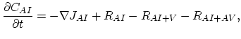 the vacancy diffusivity,
  is the thermal energy,
  is the effective valence,
  is the heat of transport, and
  is the source function that models vacancy generation and annihilation processes,
 ln ln![$\displaystyle \frac{C_V}{C_{V,0}}-(1-f)\Omega\sigma\Bigr],$](img818.png) |
(244) |
where  is the rate parameter,
  is the vacancy equilibrium concentration in the stress free crystal, and
 is the spherical part of the stress tensor.
Local vacancy migration and generation gives rise to the local volume deformation described by the kinetic relation,
![$\displaystyle \frac{\partial \varepsilon^{v}_{kk}}{\partial t}=\Omega[f \nabla \mathbf{J}_V+(1-f)G(C_V)],$](img822.png) |
(245) |
where
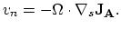 denotes the trace of the inelastic strain tensor component due to vacancy generation and migration.
Equations (4.32), (4.33) and (4.34) should be solved in conjunction with the electro-thermal equations and the stress equations [70].
denotes the trace of the inelastic strain tensor component due to vacancy generation and migration.
Equations (4.32), (4.33) and (4.34) should be solved in conjunction with the electro-thermal equations and the stress equations [70].
where
 is the total strain tensor,
  is the vacancy to atom volume proportion factor,
  and
and  are Lame's constants,
 is the bulk modulus, and
 is the displacement vector.
From the solution of these equations, considering the specific grain structure of the interconnect, we obtain two essential pieces of information.
First, we know where in the interconnect geometry void nucleation takes place, secondly we can estimate how much time is needed in the case of a given interconnect geometry and material composition to reach a critical level of tensile stress (or vacancy concentration) at the void nucleation site.
The real driving forces of the material transport flux described with (4.32) are the gradients of the electrical field
 and the mechanical stress gradient
 .
The mechanical stress gradient is the response of the interconnect metal to the electromigration stress.
If the electrical current is so small that it produces an electromigration stress small compared to the mechanical stress, no electromigration takes places.
Void nucleation occurs at the moment of equality of these two driving forces.
.
The mechanical stress gradient is the response of the interconnect metal to the electromigration stress.
If the electrical current is so small that it produces an electromigration stress small compared to the mechanical stress, no electromigration takes places.
Void nucleation occurs at the moment of equality of these two driving forces.
There has been some difference between the understanding of this sink/source function in the Sarychev model [70,84] and models developed on the basis of Korhonen's work [51,7].
Korhonen [51] assumes that the sink/source function represents the interaction of vacancies between the grain boundary and the grain: annihilation of grain boundary vacancies if their concentration is larger than equilibrium concentration, and their production in the opposite case (Section 4.4.3).
On the other hand, Sarychev [70] makes the sink/source term independent of the crystal texture and states that recombination/annihilation takes place everywhere in the bulk.
The described equation system is already solved analytically for special two-dimensional geometry cases in [70].
In [84] a simple finite element solution of the Sarychev's equations for a two-dimensional 20 m 100 m Al thin film is presented.
Next: 6 Finite Element Discretization
Up: 4 Prediction of the
Previous: 4 An Explanation of
J. Cervenka: Three-Dimensional Mesh Generation for Device and Process Simulation

