(a)
(b)
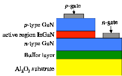
| Figure 1.1: | Schematic of a GaN based LED structure. The energy of the photon is equal to the energy gap Eg. |
GaN and its alloys with aluminum or indium are usually grown at a high temperature (approximately 1100∘C) by metal organic chemical vapor deposition or molecular beam epitaxy techniques on foreign substrates [59]. These substrates include silicon carbide for RF applications, silicon for power electronic applications, and sapphire for optical devices [54,67,73].
(a)
(b)
| Figure 1.1: | Schematic of a GaN based LED structure. The energy of the photon is equal to the energy gap Eg. |
GaN and its alloys have a wide range of optoelectronic uses because the atoms are bonded by a very ionic gallium/aluminum/indium-nitrogen chemical bond [53]. This has two important consequences.
Foremost, AlN, GaN and InN have respective direct band gap energies of 6.2 eV, 3.4 eV and 0.7 eV at room temperature [1,11], which cover the entire visible spectrum from the ultraviolet to the infrared range (see Figure 1.2). This is in contrast to (Ga,Al)As based light emitting diodes (1.5-2.2 eV) and (Al,Ga,In)P based light emitting diodes (1.3-2.5 eV) which cover only the infrared to green region [25].
The second main consequence of the strong chemical bond is their stability and resistance to degradation under high electric currents and high temperatures. Therefore, III-nitrides are widely used in laser diodes and light emitting diodes [2,56].
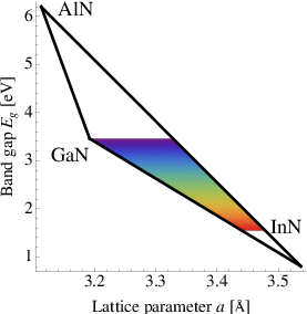
| Figure 1.2: | The band gap is shown as function of the lattice parameters. The range of visible spectrum is shown in colors. |
GaN-based laser diodes enabled the development of Blu-ray technology which has become the standard replacement of DVDs. The previous GaAs-based red laser diodes (working at λ = 650 nm) have been replaced by GaN-based laser diodes emitting blue light (λ = 405 nm) in order to store more data on every single disk due to the shorter wavelength of the writing beam [25].
A second optoelectronic application of III-nitrides are the light emitting diodes. Compared to a traditional light source, light emitting diodes have many prominent advantages including their low energy usage, long lifetime and small size, making such a light source a strong competitor in the domestic and business lighting market. Because lighting accounts for about 20% of total electricity consumption, national programs promoting light emitting diodes for lighting are underway in the US, Japan, and China. The main motivation is large-scale energy savings which would provide the benefits of reduced oil imports and lower greenhouse gas emissions [25].
(a)
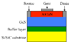
(b)
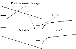
| Figure 1.3: | Schema of GaN based HEMT structure. The bi-dimensional electron gas (2DEG) is along the interface between the AlGaN and GaN layers. |
Apart from optoelectronic applications, another important III-nitride-based device is the high-electron mobility transistor. Power amplifiers based on high electron mobility transistors have demonstrated high break-down voltage, high current density, and low thermal resistance [35,83,86]. The combination of these attributes makes GaN technology attractive for continual development of high power products for applications which include commercial and military radar, electronic warfare, radio communications, and data backhaul. The above mentioned characteristics are consequences of some particular physical properties of III-nitrides [52].
An important property of III-nitrides is the strength of their chemical bond, which implies a large energy band-gap. Therefore GaN-based devices have a high breakdown field, which allows them to operate at much higher voltages than other semiconductor devices. Under such conditions, the device is subjected to high enough electric fields such that the electrons in the semiconductor can acquire enough kinetic energy to break the chemical bond (a process called voltage breakdown). If impact ionization is not controlled, it can degrade the device. Since the chemical bond is strong, III-nitride-based devices can operate at higher voltages, which are typical of higher-power applications [52].
A second consequence of the strong chemical bond is a high saturation velocity. This is the velocity of electrons at very high electric fields. High saturation velocity means that GaN devices can deliver much higher current density. The radio frequency power output is the product of the voltage and the current swings, so a higher voltage and current density can produce higher radio frequency power in a practically sized transistor. Simply put, GaN devices can produce much higher power density [52].
Low thermal resistance arises in GaN devices grown upon SiC substrates. They exhibit outstanding thermal properties, due to the high thermal conductivity of SiC. In practical terms, this means that GaN-on-SiC devices do not get as hot as GaAs or Si devices when dissipating the same power. A colder device is more reliable [52].
Let us consider the structure of a high electron mobility transistor shown in Figure 1.2. The simple structure consists of a thin AlGaN layer which is deposited on top of a thick GaN layer in order to achieve a bi-dimensional electron or hole gas at the interface between the two materials [36,68]. One of the most interesting things in GaN-based high electron mobility transistor is that a bidimensional electron or hole gas forms at the AlGaN/GaN interface without modulation doping [52]. This happens due to the spontaneous polarization and strain induced piezoelectric fields. GaN is piezoelectric because the gallium-nitrogen bond is ionic and the successive planes of gallium and nitrogen atoms are not at equal distance. When the atoms in a plane are displaced from their original position (by a mechanical pressure, for example), the planes of atoms above and below move to different positions, creating a net charge, an electric field, and a voltage. This bends the energy bands in a way that a bidimensional electron sheet is created at the interface of AlGaN/GaN or InGaN/GaN without the necessity of doping, like in Si-based transistors. Normally, the bi-dimensional carrier sheet density is around 1013∕cm2 and the mobility is around 1600 cm/Vs at room temperature [69], making GaN-based transistors fast and efficient.