(a)
(b)
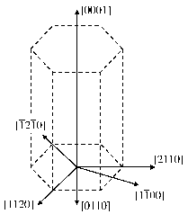
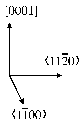
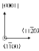
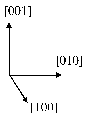
| Figure 1.4: | Directions and planes in a hexagonal lattice. |
Group III nitrides can have the following crystalline structures: the wurtzite and zinc blende. Under ambient conditions, the thermodynamically stable structure is wurtzite for bulk AlN, GaN, and InN. The zinc blende structure for GaN and InN has been stabilized by epitaxial growth of thin films on {011} crystal planes of cubic substrates such as Si, SiC, MgO, and GaAs. In these cases, the intrinsic tendency to form the wurtzite structure is overcome by topological compatibility [53].
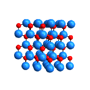
The wurtzite and zincblende structures are somewhat similar and yet different. In both cases, each group of III atoms is coordinated by four nitrogen atoms. Conversely, each nitrogen atom is coordinated by four group III atoms. The main difference between these two structures lies in the stacking sequence of closest packed diatomic planes. The wurtzite structure consists of alternating biatomic close-packed (0001) planes of Ga and N pairs, thus the stacking sequence of the (0001) plane is AaBbAa in the (0001) direction. Another way to understand the wurtzite structure is to consider the anions (N3-) forming a hexagonal close-packed structure in which the cations (Ga3+) occupy half of the tetrahedral sites [53].
The zincblende structure occurs when the hexagonal double-layers are stacked in a periodic AaBbCcAaBbCc. For AlN, GaN and InN the zincblende structure is metastable while the wurtzite variant is stable and easier to grow [25,53]. Therefore, scientific attention and industrial interest have been focused on the wurtzite form. This work considers consequently III-nitrides in their wurtzite structure.
The wurtzite group III nitrides lack an inversion plane perpendicular to the c-axis; thus, nitride surfaces have either a group III element (Al, Ga, or In) polarity with a designation of (0001)A plane or a N-polarity with a designation of (0001)B plane [53]. The distinction between these two directions is essential in nitrides because of their implications for the polarity of the polarization charge.
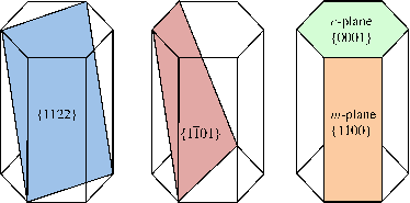
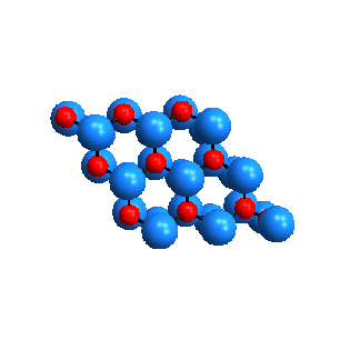
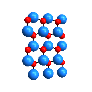
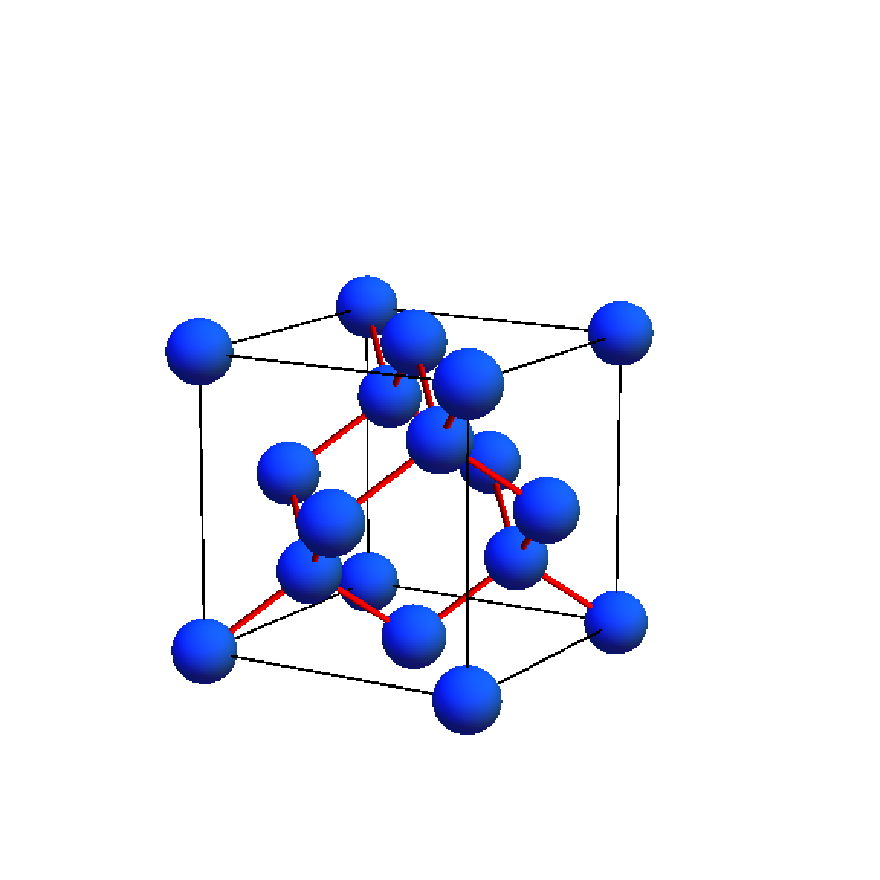
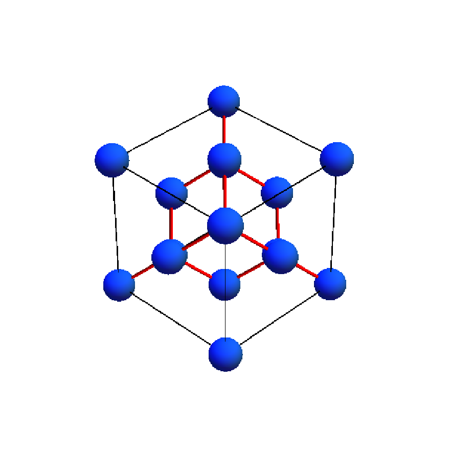
Four surfaces are of special importance in nitrides: (0001), (112), (100), and (101) planes (see Figure 1.3.1). Particular directions in hexagonal close-packed structures are ⟨0001⟩, ⟨20⟩, and ⟨100⟩ as shown in Figure 1.3.1. The (0001), or the basal plane, is the most commonly used surface for growth. The three-dimensional arrangement of wurtzite nitrides is shown in Figure 1.5 where the red color represents nitrogen atoms while blue represents the group III atom sites (Al, Ga or In).
The wurtzite structure can be represented by lattice parameters a in the basal plane and
c in the perpendicular direction, and the internal parameter u. The basal plane lattice
parameter (the edge length of the basal plane hexagon) is universally depicted by a and the
axial lattice parameter, perpendicular to the basal plane, is universally described by c. The c
parameter depicts the unit cell height. The u parameter is defined as the anion-cation bond
length (also the nearest neighbor distance or the interatomic distance) divided
by the c lattice parameter. In an ideal wurtzite structure represented by four
touching hard spheres, the values of the axial ratio and the internal parameter are
c∕a =  = 1.633 and u = 8∕3 = 0.375, respectively. The crystallographic vectors
of wurtzite are a1 = a(1∕2,
= 1.633 and u = 8∕3 = 0.375, respectively. The crystallographic vectors
of wurtzite are a1 = a(1∕2, ∕2, 0), a2 = a(1∕2,-
 ∕2, 0), c = a(0, 0,c∕a). In
Cartesian coordinates, the basis atoms are (0, 0, 0), (0, 0,u ⋅ c), a(1∕2,
∕2, 0), c = a(0, 0,c∕a). In
Cartesian coordinates, the basis atoms are (0, 0, 0), (0, 0,u ⋅ c), a(1∕2, ∕6,c∕2a), and
a(1∕2,
∕6,c∕2a), and
a(1∕2, ∕6, [u + 1∕2]c∕a) [53].
The lattice parameters of the III-nitrides are summarized in Table 1.1. Whenever a material property of the alloy is needed, for example, the lattice constant of AlxGa1-xN, Vegard’s law [76] is used in the following form:
 | (1.1) |
| Table 1.1: | The lattice constants (in Å) for GaN, AlN, InN [53], and for Si and Ge [19]. The lattice constants of AlxGa1-xN/GaN, InxGa1-xN/GaN and Si1-xGex/Si are calculated using Vegard’s law with the data in the table. |
| GaN | AlN | InN | Si(111) | Ge(111) | ||
| a | 3.22 | 3.11 | 3.54 | 5.43 | 5.65 | |
| c | 5.19 | 4.98 | 5.96 | |||
(a)

(b)
(c)
(d)
| Figure 1.5: | A 3D picture of the wurtzite structure together with some important projections [12]. |
Vegard’s law is valid only under specific conditions [76]. First principle calculations show [10] that Vegard’s law holds for AlGaN (both lattice constants) and the a-lattice constant of InGaN and AlN. Some deviations from Vegard’s law are predicted [10] for the c-lattice constant of the latter two alloys. However, since no better estimate of lattice and elastic constants is available for the whole range of compositions, Vegard’s law is used throughout this work wherever necessary [25].
| Table 1.2: | The stiffness constants (in GPa) for GaN, AlN, InN [61], for Si [29], for Ge [19] . The stiffness constants of the systems AlxGa1-xN/GaN, InxGa1-xN/GaN and Si1-xGex/Si are calculated using Vegard’s law with the data in the table. |
| c11 | c12 | c13 | c33 | c44 | c66 | ||||||||
| GaN | 374.2 | 141.4 | 98.1 | 388.6 | 98.3 | (c11-c12)∕2 | |||||||
| AlN | 410.5 | 148.5 | 98.9 | 388.5 | 124.6 | (c11-c12)∕2 | |||||||
| InN | 223 | 115 | 92 | 224 | 48 | (c11-c12)∕2 | |||||||
| Si(111) | 194.25 | 35.25 | 63.9 | 165.6 | 79.5 | 50.85 | |||||||
| Ge(111) | 155 | 21.6 | 48.2 | 128.4 | 66.7 | 40.1 | |||||||
The elastic constants of GaN, AlN, and InN are given in Table 1.2. Vegard’s law is used to calculate the constants of the ternary compounds AlxGa1-xN and InxGa1-xN. Epitaxial layers composing GaN-based devices are monocrystals. Therefore elastic anisotropy must be considered in any attempt of modeling the mechanical behavior. In order to show the importance of anisotropy, the standard deviation σY of the elastic modulus Y is calculated as a function of the x fraction for the two systems AlxGa1-xN and InxGa1-xN:
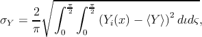 | (1.2) |
where Y i is the elastic modulus function of x in a certain direction of the 3D space. ι and ς are the angles of the polar spherical coordinate system. ⟨Y ⟩ is the average elastic modulus defined as follows:
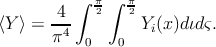 | (1.3) |
The standard deviation of the elastic modulus quantifies the dispersion from the average value. For this reason, it is an index of the anisotropy of the compounds. The comparison of σY for the three systems considered in this work is shown in Figure 1.6.
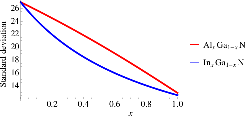
| Figure 1.6: | The standard deviation σY as function of the fraction x for the three different systems. |
Figure 1.6 shows that for all the systems the impact of the anisotropy decreases as x increases, meaning that small amounts of Al/In atoms increase strongly the effect of the anisotropy. For the wide range of composition, the standard deviation of the elastic modulus is always higher for the AlxGa1-xN system with respect to the InxGa1-xN system. As a consequence of the values of the standard deviation, elastic anisotropy is considered in the subsequent modeling.
Different types of substrates are used to grow III-nitrides depending on the application. While sapphire is mainly used for optical devices and silicon carbide for military application, silicon is preferred for civil use. A silicon substrate causes the creation of a large amount of defects and thus the resulting performance of the final devices is lower than when SiC is used. However, Si substrates are much cheaper than SiC, and this is the main factor in requests for mass production for civil application.
For growth of III-nitrides on Si, one generally starts with an AlN buffer layer and hence an AlN/Si interface. Direct growth of GaN on Si is prevented by the formation of low-melting-point Ga-Si compounds and significant diffusion of Si to the film-vapor interface resulting in the formation of SixNy therein [73]. The former results in the so-called melt-back etching, whereas the latter results in a rough interface. The presence of a defective SixNy layer has been reported at the AlN/Si interface as well. However, it does not prevent epitaxy and it is still not quite clear if it forms prior to deposition of the AlN buffer layer or during subsequent exposure of the AlN/Si interface to high temperatures during growth [73].
(a)

(b)

(c)
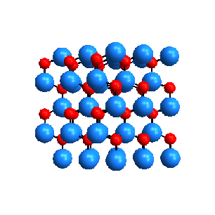
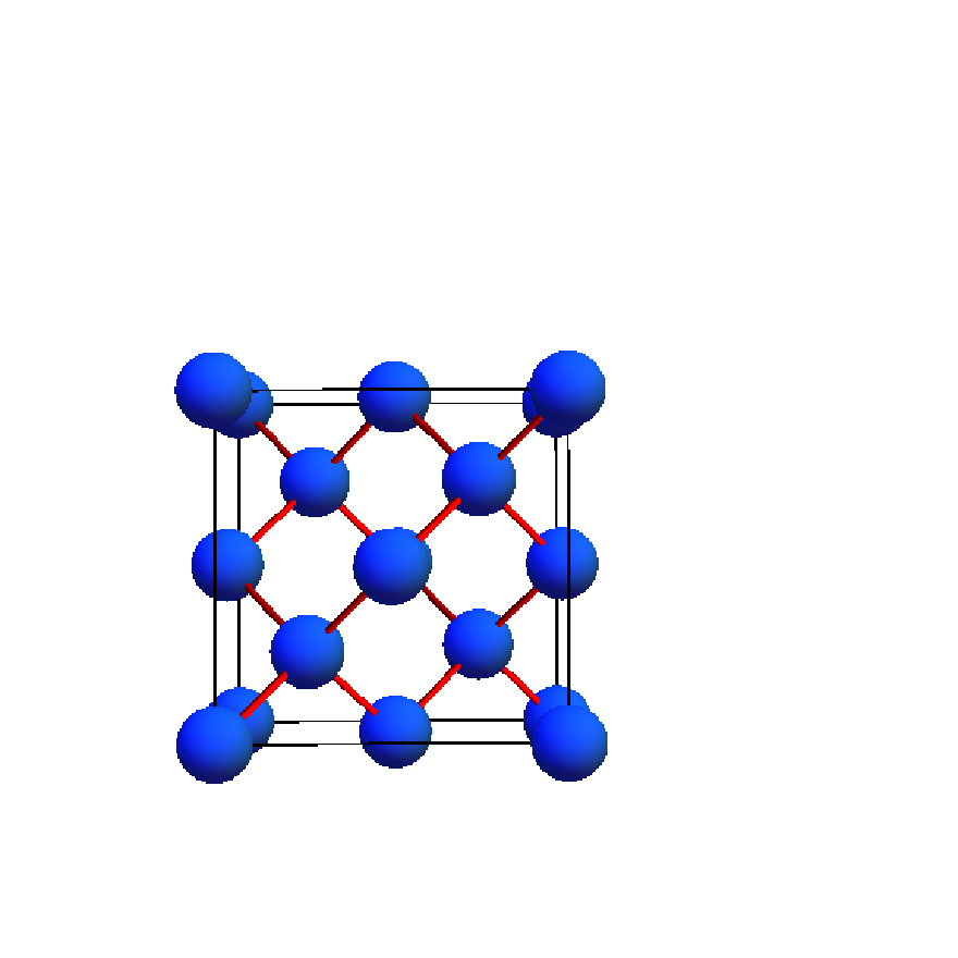
| Figure 1.7: | A 3D picture of the diamond structure together with some important projections [12]. Red lines represent the chemical bonds and the black lines are cell lines. |
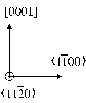
The (111) plane is the most commonly used surface of Si for growth of the III-nitrides.
The epitaxial relationship is {111}Si⟨10⟩Si ∥{0001}GaN⟨110⟩GaN. The sixfold symmetry of
arrangement of atoms on the unreconstructed {111} surface (see Figure 1.3.3) favors the
growth of the wurtzite phase with hexagonal symmetry of Ga-polarity (Ga face up).
However, the mismatch, defined as  ∕afilm, with a being the lattice
parameter, is greater than 20% for both GaN and AlN, and of a nature that would result
in tensile (or positive) stress in the film when grown directly on Si(111) [73].
Given the orientation relationship, it should be noted that for Si(111), asubstrate
should be the interatomic distance along [11] and not the often quoted lattice
parameter of Si, which is the interatomic distance along [100]. For such highly
mismatched systems, strain is very quickly relaxed by the formation of islands, i.e., the
Volmer-Weber growth mode takes place. A quick analysis of the various energies
involved in the system then provides a deeper insight into the possible growth
mode. Markov [48] determines the mechanism by which a thin film grows by
considering the chemical potentials μ of the first few n deposited layers. The chemical
potential is a function of the bond energies involved in the system. The island growth
mode, i.e., the Volmer-Weber mode, takes place when the variation of the chemical
potential within the first deposited layers dμ∕dn is negative, which corresponds to the
situation when the bond energy among the atoms of the deposited material is
higher than the bond energy between the atoms of the deposited material and
the atoms of the substrate. The Si-N bond energy of 4.5 eV [78] is lower than
the Ga-N and Al-N bond energies of 9.12 and 1.17 eV, respectively [53]. Thus,
there is no great incentive for GaN/AlN to spread out along the substrate or,
in other words, for the two-dimensional growth mode. In addition, as discussed
previously, III-nitride layers are strained, which would raise the chemical potential
of the first deposited layer with respect to the layers composing the bulk even
further.
∕afilm, with a being the lattice
parameter, is greater than 20% for both GaN and AlN, and of a nature that would result
in tensile (or positive) stress in the film when grown directly on Si(111) [73].
Given the orientation relationship, it should be noted that for Si(111), asubstrate
should be the interatomic distance along [11] and not the often quoted lattice
parameter of Si, which is the interatomic distance along [100]. For such highly
mismatched systems, strain is very quickly relaxed by the formation of islands, i.e., the
Volmer-Weber growth mode takes place. A quick analysis of the various energies
involved in the system then provides a deeper insight into the possible growth
mode. Markov [48] determines the mechanism by which a thin film grows by
considering the chemical potentials μ of the first few n deposited layers. The chemical
potential is a function of the bond energies involved in the system. The island growth
mode, i.e., the Volmer-Weber mode, takes place when the variation of the chemical
potential within the first deposited layers dμ∕dn is negative, which corresponds to the
situation when the bond energy among the atoms of the deposited material is
higher than the bond energy between the atoms of the deposited material and
the atoms of the substrate. The Si-N bond energy of 4.5 eV [78] is lower than
the Ga-N and Al-N bond energies of 9.12 and 1.17 eV, respectively [53]. Thus,
there is no great incentive for GaN/AlN to spread out along the substrate or,
in other words, for the two-dimensional growth mode. In addition, as discussed
previously, III-nitride layers are strained, which would raise the chemical potential
of the first deposited layer with respect to the layers composing the bulk even
further.
In conclusion, the chemical potential of the first GaN/AlN monolayers is higher than that of the subsequent layers. Thermodynamics indicates that in such situations III-nitrides would prefer to form multilayer islands rather than spread out as a single layer on the substrate and for that matter even on other III-nitride layers. The resultant growth mode, based on observations at a thickness greater than a bilayer, is thus the Volmer-Weber mode, involving nucleation of three-dimensional (3D) islands that then grow laterally and coalesce. It is emphasized that this discussion has been on purely thermodynamic grounds and the growth mode actually observed could be subject to kinetic modifications.
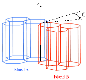
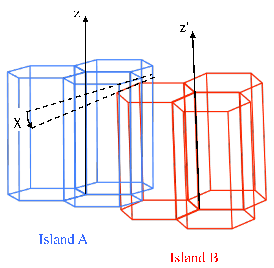
After the coalescence, the islands become domains of the continuous film. Due to different crystallographic orientation, the domains can be twisted or tilted with respect to each other to varying extents (see Figure 1.8). The consequence is that the domains are separated by low angle grain boundaries, which are composed by sets of dislocations. The difference in tilt between two domains can be accommodated by pure edge dislocations, whereas difference in twist can be accommodated by pure screw dislocations [73]. When a combination of both a difference in twist and tilt between domains exist, then all three types of dislocations (edge, screw, and mixed dislocations) would be required. Dislocations created in this way during the growth of the first III-nitride layer on Si(111) propagate through the above grown layers, reaching the active part of the device and damaging its performance. When Si is used as substrate, an extremely high density of dislocations is detected in the active part in the range between 1010-1014cm-2. X-ray diffraction (XRD) using a four-circle diffractometer [51], TEM [51], and atomic force microscopy (AFM) [58] are the three most commonly used techniques to characterize these dislocations.
(a)
(b)
| Figure 1.8: | The islands A and B separated by a pure tilt boundary represented by the angle ζ and a pure twist boundary represented by the angle χ. |