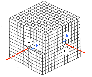
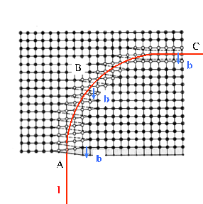
| Figure 1.9: | Changing dislocation type along a single dislocation line with Burgers vector b: screw-type (A), mixed-type (B) and edge-type (C) [80]. |
III-nitride films on Si are host to all major defect types including point defects, line defects or dislocations, plane defects, such as stacking faults, inversion domains and cracks, and 3D defects, such as V-shaped pits and pipes [53]. Despite defects affecting both device performance and lifetimes, III-nitride-on-Si devices have been commercialized in the last decade [73]. Extensive research has thus been devoted to understanding the origin, structure, and evolution of defects during growth.
Of the defects mentioned above, III-nitride devices stand apart because of their high density of dislocations. Dislocations propagate through the bulk of the heterostructure and reach the core part of the device. There they form new energy levels inside the energy band. Electrons can be trapped in these energy levels by reaching a lower energy state and thus damaging the electrical performance of the device. In addition, the evolution of dislocation configuration during growth alters the strain-stress fields of the structure. This is a second cause for the modification of the band structure.
The dislocation density in 1μm thick GaN layers grown on Si(111) is typically 1010cm-2 at the surface of the film, and the corresponding number for films grown on sapphire and SiC is 108cm-2. It is important to note the role of film thickness, as dislocation density is not a constant but varies across the film. Considering a structure composed by a GaN film grown upon an AlN layer on a Si(111) substrate, at the GaN/AlN interface the dislocation density can be in excess of 1014cm-2 and its reduction with thickness depends on the process type and the device structure. A particular type of growth technique called lateral growth technique reduces the dislocation density to about 106cm-2 [21] but this is still about two orders of magnitude higher than the value found in GaAs-based devices.
A dislocation is a line defect in a crystal, which can greatly affect its material properties. A dislocation is usually represented by an oriented dislocation line, l, and characterized by its Burgers vector, b, describing displacements introduced in the crystal by the dislocation [25].
A dislocation can not end within a crystal and it is contained within a crystal only as a complete loop. Otherwise, the dislocation line can end at the material surface.
Based on the relationship of l and b, three dislocation types are distinguished (see Figure 1.9): an edge-type dislocation with l ⊥ b, a screw-type dislocation with l ∥ b, and a mixed-type dislocation (b ∦ l ⁄⊥ b). The dislocation type can change as the dislocation line changes its direction in the crystal. This is because the Burgers vector b is a constant characteristic of a dislocation which remains unchanged along the whole single dislocation line. It is worth noting that the orientation of b in the standard definition (Burgers-Frank or a continuous elasticity definition [9]) depends on the actual orientation of the dislocation line l: an opposite dislocation line direction -l yields an opposite orientation of the Burgers vector -b. However, the uncertainty in sign of b and l does not affect their mutual relation in terms of defining an edge, screw or mixed type dislocation.
| Figure 1.9: | Changing dislocation type along a single dislocation line with Burgers vector b: screw-type (A), mixed-type (B) and edge-type (C) [80]. |
The Burgers vector of a perfect dislocation is a lattice vector. As such, there are three basic types of dislocations in III-nitrides according to the Burgers vector: a-type dislocations with b = 1∕3⟨110⟩, c-type dislocations with b = ⟨0001⟩, and (a + c)-type dislocations with l = 1∕3⟨23⟩. It is important to distinguish between these two nomenclatures: an a-type dislocation can be either an edge, screw or mixed dislocation depending on the actual dislocation line direction. Since the Burgers vector cannot change along the dislocation line, the latter terminology is used in this text for describing dislocation types.