


Next: 2.3 Carrier Generation and
Up: 2. Simulation of Semiconductor
Previous: 2.1 Classical Semiconductor Device
Subsections
2.2 Analytic MOSFET Approximations
For the simulation of electronic circuits it is often of interest to have
compact models for the involved devices. In comparison to solving the
semiconductor device equations using compact models reduces the simulation time
drastically. Compact models can also be a good guide on what effects the
change of physical quantities has on the device characteristics.
The disadvantage is that for each device the right model has to be chosen and
the according model parameters have to be extracted. Furthermore, it is not
possible to investigate novel device geometries or new materials without
processing the device and obtaining an adequate model first.
2.2.1 Interface and Oxide Charges
A change in the interface and oxide charges (
 and
and
 )
contributes to a threshold voltage shift
)
contributes to a threshold voltage shift
 as
as
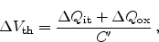 |
(2.31) |
where  is the capacitance per unit area of the oxide.
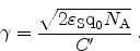
In the context of NBTI interface charges are usually the result of charged
interface defects
 . The interface charge depends on the Fermi-level
 and the trap occupancy
  and can be calculated
as [4]
and can be calculated
as [4]
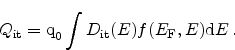 |
(2.32) |
Charged oxide traps
 contribute to the threshold voltage shift depending
on their position in the dielectric. The resulting, effective,
contribute to the threshold voltage shift depending
on their position in the dielectric. The resulting, effective,
 can be
evaluated as [5]
can be
evaluated as [5]
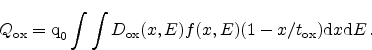 |
(2.33) |
Here,
 is the oxide thickness.
A very common compact model for the MOSFET is the Level 1 model implemented in
the circuit simulator SPICE. There the threshold voltage is obtained as
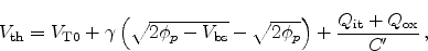 |
(2.34) |
where  is the threshold voltage for
 V and
V and  the
body-effect parameter, defined as
the
body-effect parameter, defined as
 |
(2.35) |
Here,
 is the permittivity of the silicon substrate and
 the acceptor doping concentration. The potential in the neutral
p-type region
the acceptor doping concentration. The potential in the neutral
p-type region  is evaluated as
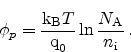 |
(2.36) |
During NBTI stress this threshold voltage is shifted due to trapped charges by
obtained from (2.31).
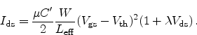
In the linear regime, where
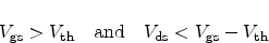 |
(2.37) |
the drain current is obtained as
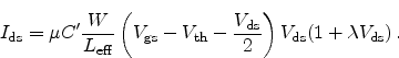 |
(2.38) |
Here,  is the effective carrier mobility,
  the device width,
 the effective gate length, and
  is an empirical
parameter reflecting the channel length modulation.
is an empirical
parameter reflecting the channel length modulation.
In the saturation regime, where
|
(2.39) |
the drain current is modeled as
 |
(2.40) |
In NBTI investigations the degradation of the transconductance
 is an
important figure of merit. The transconductance is defined as the change of
drain current as a result of a change in the gate voltage
is an
important figure of merit. The transconductance is defined as the change of
drain current as a result of a change in the gate voltage
 |
(2.41) |
Devine et al. proposed a transconductance shift versus interface trap
(
 ), relation as [6]
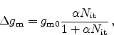 |
(2.42) |
where  is a processing related parameter. As mobility model Devine
proposed
is a processing related parameter. As mobility model Devine
proposed
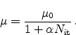 |
(2.43) |
With respect to modeling of NBTI these equations show very well how, for
example, a reduction of the carrier mobility reduces the drain current, as does
an increase of the threshold voltage.
Next: 2.3 Carrier Generation and
Up: 2. Simulation of Semiconductor
Previous: 2.1 Classical Semiconductor Device
R. Entner: Modeling and Simulation of Negative Bias Temperature Instability