


Next: 2.2 Analytic MOSFET Approximations
Up: 2. Simulation of Semiconductor
Previous: 2. Simulation of Semiconductor
Subsections
2.1 Classical Semiconductor Device Equations
The semiconductor device equations can be used to describe the whole simulation
domain of a semiconductor device. They are applied to the bulk semiconductor,
the highly doped regions such as source and drain, and to dielectric regions
such as the gate dielectric. In this section the classical semiconductor
device equations are presented which are widely used for device simulation and
their derivation.
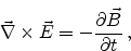
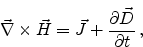
The equations developed by James Clerk Maxwell describe the behavior of
electric and magnetic fields and their interaction with matter. They were
published by Maxwell in 1864 [2] and in its original form
comprised of 20 equations in 20 unknowns. Later they were reformulated in
vector notation to the following form
 |
(2.1) |
 |
(2.2) |
 |
(2.3) |
 |
(2.4) |
Here,  is the electric field,
  the magnetic field,
 the displacement vector, and
  the magnetic flux density
vector.
the magnetic flux density
vector.  denotes the conduction current density,
  is the
electric charge density, and
is the
electric charge density, and
 is the partial derivative
with respect to time.
is the partial derivative
with respect to time.
Equation (2.1) expresses the generation of an electric field due to a
changing magnetic field (Faraday's law of induction), (2.2) predicts the
absence of magnetic monopoles (magnetic sources or sinks), (2.3)
reflects how an electric current and the change in the electric field produce a
magnetic field (Ampere-Maxwell law), and finally (2.4) correlates the
creation of an electric field due to the presence of electric charges (Gauss'
law).
We are using the Maxwell's equations to derive parts of the semiconductor
device equations, namely the Poisson equation and the continuity equations.
2.1.2 Poisson's Equation
Poisson's equation correlates the electrostatic potential  to a given
charge distribution . It can be derived from (2.4) using the
relation between the electric displacement vector and the electric field
vector,
to a given
charge distribution . It can be derived from (2.4) using the
relation between the electric displacement vector and the electric field
vector,
 |
(2.5) |
where
 is the permittivity tensor. This relation is valid
for materials with time independent permittivity. As materials used in
semiconductor devices normally do not show significant anisotropy of the
permittivity,
can be considered as a scalar quantity
is the permittivity tensor. This relation is valid
for materials with time independent permittivity. As materials used in
semiconductor devices normally do not show significant anisotropy of the
permittivity,
can be considered as a scalar quantity
 in device simulation. The total permittivity is obtained from
the relative
in device simulation. The total permittivity is obtained from
the relative
 and the vacuum permittivity
 as
as
 .
Table 2.1 gives an overview of relative permittivity constants for some
materials commonly used in semiconductor devices.
.
Table 2.1 gives an overview of relative permittivity constants for some
materials commonly used in semiconductor devices.
Table 2.1:
Relative permittivity constants for materials used in or considered
for semiconductor devices.
| Material |
Relative Permittivity |
| Si |
11.7 |
| GaAs |
12.5 |
| Ge |
16.1 |
SiO |
3.9 |
| HfO |
 25 25 |
HfSiO |
15-18 |
| ZrO |
20-25 |
|
As
 for the stationary case can be expressed as a
gradient field of a scalar potential field
for the stationary case can be expressed as a
gradient field of a scalar potential field
 |
(2.6) |
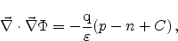
Substituting (2.5) and (2.6) in (2.4) we get
 |
(2.7) |
As we consider the permittivity a scalar, which is constant in homogeneous
materials, we obtain Poisson's equation
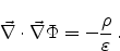 |
(2.8) |
The space charge density consists of
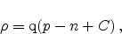 |
(2.9) |
where q is the elementary charge,  and
and  the hole and electron
concentrations, respectively, and
the hole and electron
concentrations, respectively, and  the concentration of additional,
typically fixed, charges. These fixed charges can originate from charged
impurities of donor (
the concentration of additional,
typically fixed, charges. These fixed charges can originate from charged
impurities of donor (
 ) and acceptor (
 ) type and from trapped holes
(
) type and from trapped holes
( ) and electrons (
 ),
),
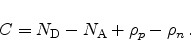 |
(2.10) |
The inclusion of trapped carriers is important for the simulation of the impact
of degradation on the device performance (Section 2.2,
Section 5.3.2, Chapter 6).
Together (2.8) and (2.9) lead to the form of Poisson's
equation commonly used for semiconductor device simulation
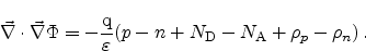 |
(2.11) |
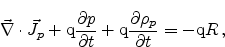
The continuity equations can be derived from (2.3) by applying the
divergence operator,
 , to the equation and considering that the
divergence of the curl of any vector field equals zero
, to the equation and considering that the
divergence of the curl of any vector field equals zero
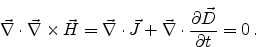 |
(2.12) |
Separating the total current density into hole and electron current
densities,
 , and using (2.4) and
(2.9) gives
, and using (2.4) and
(2.9) gives
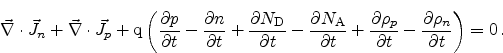 |
(2.13) |
When we consider the charged impurities as time invariant and introduce a
quantity  to split up (2.13) into separate equations for electrons
and holes, we get
to split up (2.13) into separate equations for electrons
and holes, we get
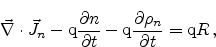 |
(2.14) |
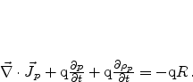 |
(2.15) |
The quantity gives the net recombination rate for electrons and holes. A
positive value means recombination, a negative value means generation of
carriers. Models for are presented in Section 2.3.
There are two major effects which lead to current flow in silicon. First, the
drift of charged carriers due to the influence of an electric field, and
second, the diffusion current due to a concentration gradient of the carriers.
Charged carriers in a semiconductor subjected to an electric field are
accelerated and acquire a certain drift velocity. The orientation depends on
the charge state, holes are accelerated in direction of the electric field and
electrons in opposite direction. The magnitude of the drift velocity depends
on the statistical probability of scattering events. At low impurity
concentration, the carriers mainly collide with the crystal lattice. Is the
impurity concentration higher the collision probability with the charged
dopants through Coulomb interaction becomes more and more likely, thus reducing
the drift velocity with increasing doping concentration.
For low electric fields, the drift component of the electric current can be
expressed in terms of Ohm's law as
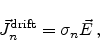 |
(2.16) |
 |
(2.17) |
Here,  denotes the conductivity and can be expressed in terms of
carrier mobilities for electrons and holes,
denotes the conductivity and can be expressed in terms of
carrier mobilities for electrons and holes,  and
and
 , as
, as
 |
(2.18) |
 |
(2.19) |
The mobility for electrons is, due to their lower effective mass, about three
times higher than for holes.
A concentration gradient of carriers leads to carrier diffusion. This is
because of their random thermal motion which is more probable in the direction
of the lower concentration. The current contribution due to the concentration
gradient is written as
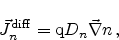 |
(2.20) |
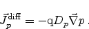 |
(2.21) |
Here,  and
and  are the diffusion coefficients for electrons and holes,
which can, in thermal equilibrium for non-degenerate semiconductors, be
expressed in terms of the mobility using the Einstein relation
are the diffusion coefficients for electrons and holes,
which can, in thermal equilibrium for non-degenerate semiconductors, be
expressed in terms of the mobility using the Einstein relation
 |
(2.22) |
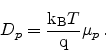 |
(2.23) |
Combining the current contributions of the drift and the diffusion effect we
get
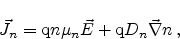 |
(2.24) |
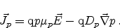 |
(2.25) |
With the Poisson equation (2.11), the continuity equations for
electrons and holes (2.14) (2.15), and the drift-diffusion
current relations for electron- and hole-current (2.24) (2.25) we now
have a complete set of equations which can be seen as fundamental for the
simulation of semiconductor devices:
 |
(2.26) |
|
(2.27) |
 |
(2.28) |
|
(2.29) |
|
(2.30) |
These equations, not including the charge contribution of trapped carriers,
have first been published by VanRoosbroeck in 1950 [3].
This set of equations is widely used in numerical device simulators and
provides only the basics for device simulation. In modern simulators they are
accompanied by higher order current relation equations like the hydrodynamic,
six-, or eight-moments models. There are models for the carrier mobility, the
carrier generation and recombination (Section 2.3), for quantum
effects like quantum mechanical tunneling (Section 5.3) or quantum
confinement (Section 2.4.1) and of course for modeling of device
degradation, as negative bias temperature instability (Chapter 6).
Next: 2.2 Analytic MOSFET Approximations
Up: 2. Simulation of Semiconductor
Previous: 2. Simulation of Semiconductor
R. Entner: Modeling and Simulation of Negative Bias Temperature Instability