


Next: 3.2 Centers
Up: 3. The Silicon/Silicon-Dioxide Interface
Previous: 3. The Silicon/Silicon-Dioxide Interface
Subsections
3.1 Silicon Dangling Bonds
Figure 3.1:
(a) At the silicon surface silicon atoms are missing and unpaired
valence electrons exist forming electrically active interface traps. (b)
After oxidation most interface states are saturated with oxygen bonds. (c)
After annealing the surface with a hydrogen related species the amount of
interface defects is further decreased.
![\includegraphics[width=0.32\textwidth]{figures/si-surface}](img319.png)
Silicon surface
|
![\includegraphics[width=0.32\textwidth]{figures/si-sio2-unpassivated}](img320.png)
Unpassivated
 interface
|
![\includegraphics[width=0.32\textwidth]{figures/si-sio2-passivated}](img321.png)
After hydrogen passivation
|
|
The silicon atom possesses four valence electrons and therefore requires four
bonds to fully saturate the valence shell. In the crystalline structure each
silicon atom establishes bonds to its four neighboring atoms, leaving no
unsaturated bond behind. At the surface of the silicon crystal atoms are
missing and traps are formed as shown in Figure 3.1(a). The density of
these interface states,
 , in this regime is approximately
 cm
cm eV
eV . After oxidation most interface states are
saturated with oxygen atoms (Figure 3.1(b)). The density is then
approximately
. After oxidation most interface states are
saturated with oxygen atoms (Figure 3.1(b)). The density is then
approximately
 cmeV [16].
This number is already a major improvement of the interface quality. But in an
MOS transistor with a gate length of 100nm and a gate width of 1 m this
density still translates to 1000 dangling bonds. With such a high number of
interface defects a transistor would still not operate properly. Therefore, it
is mandatory to increase the quality of the
interface in MOS device
technology as much as possible. Each electrically active interface state leads
to degradation of important transistor parameters such as the threshold
voltage, the on-current, or the surface carrier mobility. To further improve
the interface, the number of dangling valence bonds is further reduced by
annealing the interface in forming gas with hydrogen atoms, as shown in
Figure 3.1(c). The dangling silicon bonds are passivated by
forming Si-H bonds. With this treatment the amount of electrically active
interface states can be reduced to around
m this
density still translates to 1000 dangling bonds. With such a high number of
interface defects a transistor would still not operate properly. Therefore, it
is mandatory to increase the quality of the
interface in MOS device
technology as much as possible. Each electrically active interface state leads
to degradation of important transistor parameters such as the threshold
voltage, the on-current, or the surface carrier mobility. To further improve
the interface, the number of dangling valence bonds is further reduced by
annealing the interface in forming gas with hydrogen atoms, as shown in
Figure 3.1(c). The dangling silicon bonds are passivated by
forming Si-H bonds. With this treatment the amount of electrically active
interface states can be reduced to around
 cmeV.
cmeV.
This is an acceptable number and a first-class
interface can be
formed. Ironically, exactly these Si-H bonds are the cause for NBTI, as
extensively described in Chapter 6. The bonds can break at elevated
temperatures and high electric fields due to their lower binding energy and
re-activate the interface states.
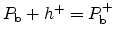
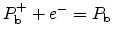
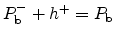
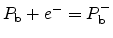
The exact properties of the interface defects, which are trivalent silicon
atoms with one unpaired valence electron
 |
(3.1) |
or
 |
(3.2) |
depends on the exact atomic configuration and on the orientation of the
substrate. While
 centers (3.1) are formed on (111)
oriented substrates,
centers (3.1) are formed on (111)
oriented substrates,
 (3.1) and
 (3.2) centers can
only exist on (100) orientations. Figures 3.2 and
3.3 depict the atomic configurations of all three trap
types.
(3.2) centers can
only exist on (100) orientations. Figures 3.2 and
3.3 depict the atomic configurations of all three trap
types.
Figure 3.2:
defect located at a
interface with (111) orientation.
The defect is formed by an unpaired valence electron of a silicon atom
back-bonded to three other silicon atoms. The defect's trap energy lies in
the silicon band-gap. Thus, the charge state of the trap depends on the
Fermi-level and it is electrically active [17].
|
|
Figure 3.3:
and
defects located at a
interface with (100)
orientation. The
center is back-bonded to three silicon atoms and
electrically very similar to the
center. The silicon atom of the
center is back-bonded to two other silicon atoms and an oxygen atom.
Both traps are electrically active as their energy lies in the silicon
band-gap making their charge state Fermi-level dependent [17].
|
|
Recent works show [18,19,20] that all three types
of
centers give rise to trap levels in the silicon band-gap. The charge
state of the traps therefore depends on the Fermi-level.
3.1.1 Amphoteric Nature of Dangling Bonds
All three types of silicon dangling bonds investigated up to now (
,
, and
) are reported to be of amphoteric nature. Their energy
distribution comprises of two distinct peaks in the silicon band-gap, as seen
in Figure 3.6.
The two peaks have different properties regarding their possible charge states
and their energetic positions depend on the type of the trap center. For
and
these are:
- Donor-like energy levels: They are located in the lower half of the
band-gap around 0.25eV [21] above the valence band edge.
The trap levels are positively charged when empty and electrically neutral
when occupied by an electron. In the empty state they are diamagnetic, a
very weak form of magnetism triggered by an external magnetic field changing
the orbital motion of the atoms core electrons. With one unpaired electron
the trap levels are paramagnetic, a stronger form of magnetism initiated by
the presence of a magnetic field and unpaired electrons. The possible charge
states of the
centers can be written as
 and
and
 .
.
- Acceptor-like energy levels: They are located in the upper half of the
band-gap, around 0.85eV [21] above the valence band. The
trap levels are electrically neutral when empty and negatively charged when
occupied by an electron. They are therefore paramagnetic when empty (the
same state as the filled donor like level, with one electron in the
center), and diamagnetic when occupied, as the total amount of electrons in
the
center is then two. The charge states are
 and
and
 .
.
centers have the same, amphoteric nature but the energy levels of the
peaks are different, as shown in Figure 3.6(b).
Figure 3.4:
Energy diagram of a
center at the
interface in weak
inversion. The trap consists of donor like states in the lower and
acceptor like states in the upper half of the band-gap due to its
amphoteric nature. The Fermi-level determines the filling and therefore
the charge state. In this configuration the trap is slightly positively
charged.
|
|
Figure 3.4 illustrates the determination of the charge state of an
amphoteric interface trap in weak inversion. At these conditions the upper
peak is totally empty and therefore electrically neutral. The lower peak is
filled to approximately two thirds and positively charged.
3.1.2 Characterization of Trap Centers
A tool with the analytical power and sensitivity to identify the atomic-scale
structure of the different traps is the electron spin resonance (ESR)
measurement [22,23]. The ESR measurement is suited to
investigate the NBTI induced interface state
generation [24,25,23]. The draw-back is that after
stressing the device at the poly-gate with high voltages, the gate has to be
etched off before ESR measurements can be performed. For the investigation of
fully processed devices the spin-dependent recombination (SDR) technique can be
used [26,27].
The SDR technique can be explained by using the Shockley-Read-Hall (SRH) model
(Section 2.3.2) for recombination and the Pauli exclusion principle as
follows [28]. The device under test (DUT) is operated as a gate
controlled diode with the source/drain to substrate slightly forward biased.
With this forward bias the current is dominated by recombination at the trap
centers of the
interface. At a certain gate voltage the recombination
current has its maximum, as determined by the DCIV method described in
Section 4.2. The DUT is exposed to a large DC magnetic field which is slowly
varied to partially align the spins of the paramagnetic charge carriers and the
paramagnetic trapping centers. Because of the Pauli exclusion principle it is
not possible that a carrier is trapped by a trap having the same spin
orientation. When the ESR condition is satisfied, the electron spins are
flipped. This increases the probability of different spin orientations for
carriers and traps and therefore increases the measured recombination current.
This spin dependent increase in recombination current is evaluated in SDR.
Figure 3.5:
Energy distribution,
, of traps at the (111)
interface after Ragnarsson et al. [21]. The two peaks of
Gauss'ian form are observed in the upper and lower half of the band-gap.
After annealing at zero and -0.8 V bias the trap density is reduced.
|
|
Early works [29,16,30] concentrated on the
investigation of (111) oriented substrates, mainly due to the higher
defect density compared to other wafer orientations and therefore easier
experimental evaluation. Figure 3.5 gives the energy distribution of the
interface trap density
for
centers at (111) oriented
interfaces after Ragnarsson [21]. It can be seen that the
interface trap energies are spread according to a Gauss'ian peak in the upper
and another peak in the lower half of the band-gap. During passivation with
hydrogen at elevated temperatures of 170 ^C the electrically active dangling
bonds are saturated with hydrogen atoms. The peaks of the maximum trap
concentration stay approximately at the same energy levels whereas the
concentration decreases continuously.
Figure 3.6:
Estimated density-of-states (DOS) distributions of (a)
and (b)
centers at the (100)
interface. The data are from
Lenahan et al. [20] and give only a ``crude, semi-quantitative
estimation'' as precise measurements are not yet available. Important
details are the broader distribution of the
centers and the
distribution of most
levels within the
levels.
|
|
Recent works [19,21,20,18,31]
concentrate on the technologically much more important (100) substrate
orientation. The standard silicon CMOS processes of most applications use this
crystal orientation. The
defects found at interfaces of this wafer
orientation are very similar to the
centers found at (111)
interfaces. The
centers, in contrast, are found to comprise of
completely different levels in energy. Lenahan et al. [20] gives
an estimation of the energy distribution of
and
centers, as seen
in Figure 3.6.
The number of
centers is assumed to be lower than that of
centers. Still, around the peak levels of the
centers a small change in
the Fermi-level can have a significant impact on the charge state because of
these
centers and their narrow distribution.
Although the density of silicon dangling bonds is rather small, they still lead
to worse device characteristics. Therefore, it is of major interest to reduce
the amount of electrically active interface traps as much as possible.
It has been shown that by subjecting the MOS device to a post metallization
anneal or to a forming gas anneal, the density of electrically active traps can
be reduced dramatically. As a model for the passivation process the reactions
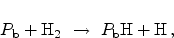 |
(3.3) |
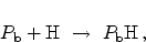 |
(3.4) |
have been suggested in the
literature [32,33,34,35].
The electrical activity of the
center is eliminated by a hydrogen atom as
it shifts the energy levels of the trap out of the silicon
band-gap [16], and thus passivates the defect.
During the negative bias temperature (NBT) stress exactly these hydrogen
passivated silicon bonds can be broken. Broken bonds have, again, electrically
active states in the band-gap which lead to additional charge on the interface
and thus to degradation of important transistor parameters, as described in
detail in Chapter 6.
Next: 3.2 Centers
Up: 3. The Silicon/Silicon-Dioxide Interface
Previous: 3. The Silicon/Silicon-Dioxide Interface
R. Entner: Modeling and Simulation of Negative Bias Temperature Instability
![\includegraphics[width=16cm]{figures/pb-center}](img328.png)
![\includegraphics[width=16cm]{figures/pb0-pb1-centers}](img329.png)
![\includegraphics[width=10cm]{figures/pb-schematic}](img334.png)
![\includegraphics[width=\figwidth]{figures/dit-dos-ragnarsson00}](img335.png)
![\includegraphics[width=0.495\textwidth]{figures/pb0-dos}](img336.png)
![\includegraphics[width=0.495\textwidth]{figures/pb1-dos}](img337.png)