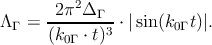
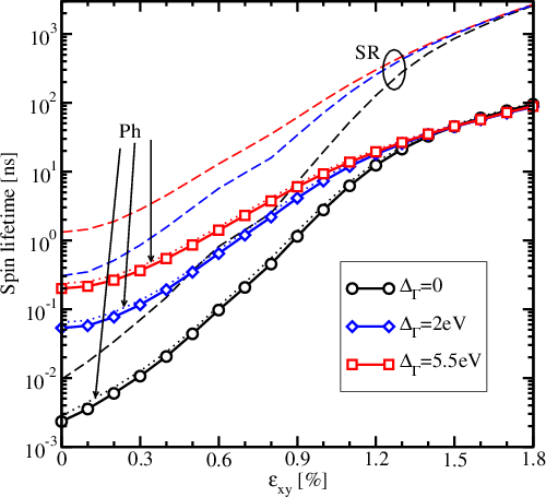
The [001] equivalent valley coupling through the Γ-point results in a subband splitting in confined electron structures [87]. This subband splitting is not limited to strained structures and thus must be taken properly into account for the calculation of the spin lifetimes in relaxed structures as well. The valley splitting in a silicon quantum well at zero strain as a function of the quantum well width has been studied for a long time. The expression for the valley splitting can be written as [55]
|
| (4.45) |
where Δ
The values of the valley splitting obtained from a 30-band
one can reproduce the corresponding data. Both methods reproduce the features of the conduction and valence band equally well, but require additional experimental verification at higher energies where discrepancies appear.
Once Λ
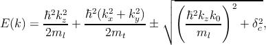 | (4.46) |
with
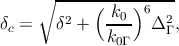 | (4.47) |
where
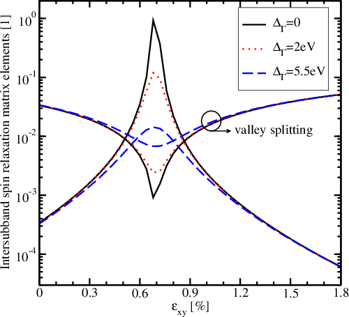
The surface roughness induced normalized and squared intersubband spin
relaxation matrix element
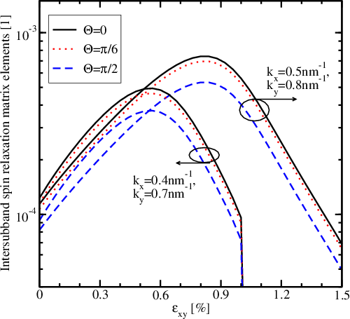
Figure 4.24 describes how
The variation of the surface roughness (
In order to understand this behavior, the spin-flip caused by the intra- and
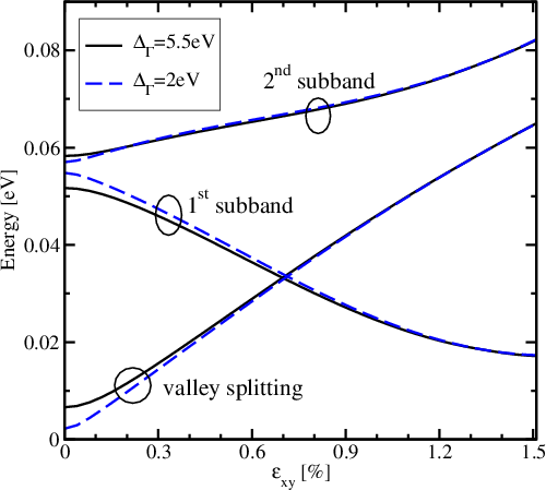
intervalley transitions needs to be analyzed. Figure 4.26 shows the energy levels of
the two lowest unprimed subbands, which are primarily responsible for the spin
relaxation at the different Δ