5.3 Solution
5.3.1 Solution with Charge Neutrality Constraint
Analytical Approach
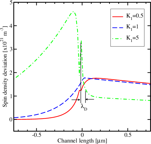
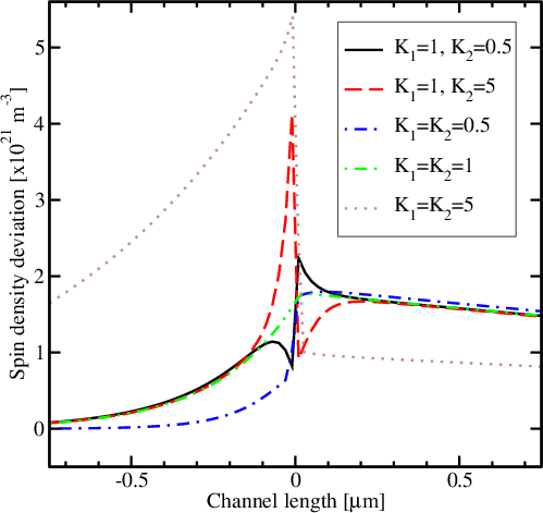
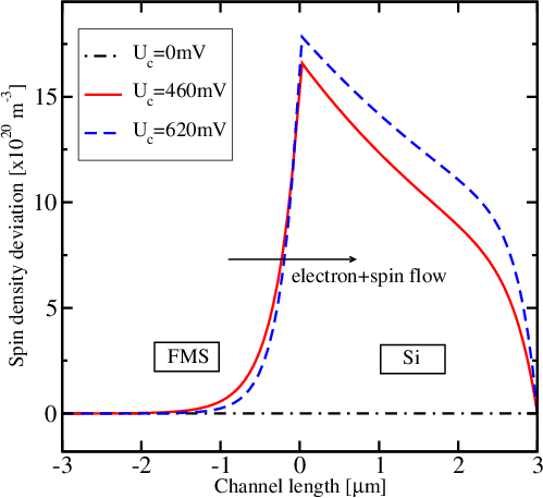
When the charge current flows through the interface, the spin accumulation in the
semiconductor appears. When K1=K2=1 (c.f. Table 5.1), the charge neutrality is
restored. To solve the spin transport equations analytically for the structure
shown in Figure 5.2, the general solution for the spin density deviation δs in
both the FMS and the Si sides must be assumed according to [173, 190]
 | (5.31a) |
 | (5.31b) |
where a1(a2) and b1(b2) are the constants. The spin density can be expressed
as s = δs + (n↑eql - n
↓eql) (c.f. Equation 5.18a to Equation 5.18c). The electron
concentration is n = ND. Based on these two, one can derive the up- and
down-spin concentrations and the spin current density (Js) as well from
Equation 5.22a and Equation 5.22b.
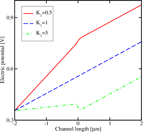
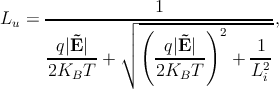
The external electric field (Ẽ) modifies the intrinsic spin diffusion length Li in
any semiconductor [173]. Two distinct spin diffusion lengths (Lu is the up-stream,
and Ld is the down-stream) characterize the spin motion, and those strongly
depend on Ẽ
 | (5.32a) |
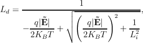 | (5.32b) |
which is related to the intrinsic spin diffusion length Li by
 | (5.33) |
Li is related to the spin relaxation time via [173]
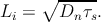 | (5.34) |
In order to solve the transport equations, one can formulate the boundary
conditions as elucidated below.
- In a doped semiconductor with homogeneous carrier concentration the
up(down)-spin chemical potential [173, 174, 181], represented by M↑ (M↓),
is related to its concentration. The spin chemical potential remains
continuous at the interface, hence [173]
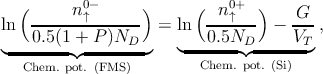 | (5.35a) |
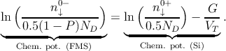 | (5.35b) |
Here, G is a constant describing as the spin chemical potential drop at the
interface, and is responsible for spin injection from the FMS to the Si side.
Therefore, G must depend on both the bulk spin polarization P and the
electric field Ẽ.
- In the language of chemical potentials, the expression for the up(down)-spin
current density can be reformulated as [173, 190]
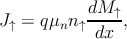 | (5.36a) |
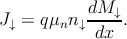 | (5.36b) |
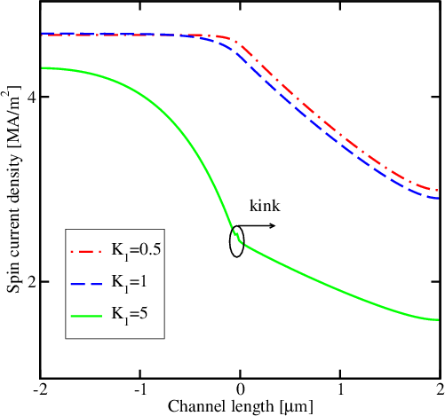
As the up(down)-spin current density J↑ (J↓) is continuous at the interface,
the above equations yield to
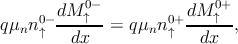 | (5.37a) |
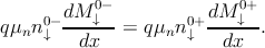 | (5.37b) |
- The spin density deviation δs is zero at the left and the right boundary,
maintaining the thermal equilibrium. Hence,
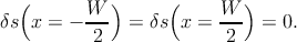 | (5.38) |
In order to derive the solution for the spin deviation and the spin current
density, one must solve for 5 unknown parameters viz. a1, a2, b1, b2, and G. The
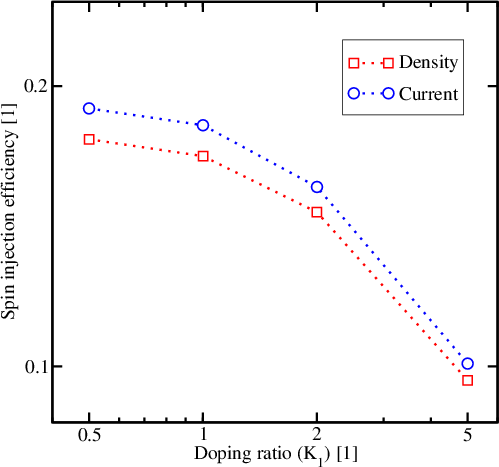
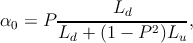
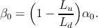
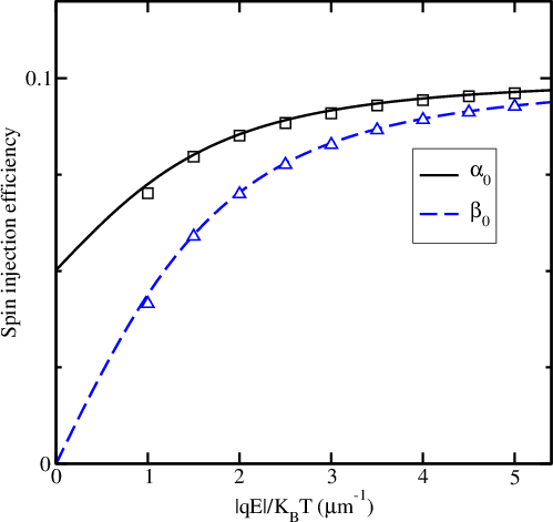
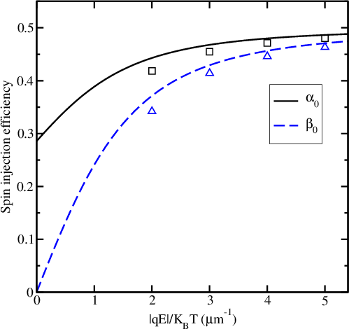
spin injection efficiency can be formulated from two different approaches [173],
one by the polarization of the spin current density (α) and the other by the
polarization of the spin density (β)
 | (5.39) |
 | (5.40) |
Therefore, at the silicon junction, α0 =  and β0 =
  .
.
The analytical expressions for α0 and β0 are cumbersome. The simplified
expressions, valid for lower values of the bulk spin polarization P are [190]
 | (5.41) |
 | (5.42) |
The expression for constant G is
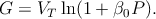 | (5.43) |
Equation 5.42 indicates that α0 is always larger than β0 irrespective of the value of
the applied field. If the electric field is very small, both the up- and down-spin
diffusion lengths Lu and Ld tend to the intrinsic value and hence from
Equation 5.41, α0 → . This also means β0=0 and from Equation 5.43 G=0. At
the strong field limit, the electrons move with the drift velocity and so does the
spin polarization [173]. Ld is simply the distance over which the carriers
move within the spin lifetime. Thus, when the electric field increases,
Ld →
. This also means β0=0 and from Equation 5.43 G=0. At
the strong field limit, the electrons move with the drift velocity and so does the
spin polarization [173]. Ld is simply the distance over which the carriers
move within the spin lifetime. Thus, when the electric field increases,
Ld →

 Li2, L
u →
Li2, L
u →

 [173]. This makes the ratio

 →0 as Ẽ →∞,
and both α0 and β0 tend to reach a saturation value fixed by the bulk spin
polarization P at the ferromagnetic semiconductor. The maximum and minimum
values of the mentioned parameters are listed in Table 5.2. Therefore,
for small values of P, the spin injection efficiency in Si can be predicted
analytically.
→0 as Ẽ →∞,
and both α0 and β0 tend to reach a saturation value fixed by the bulk spin
polarization P at the ferromagnetic semiconductor. The maximum and minimum
values of the mentioned parameters are listed in Table 5.2. Therefore,
for small values of P, the spin injection efficiency in Si can be predicted
analytically.


 and
and 

 through the bar (
 =2
=2