1.3 NBTI Experiments
In the past, a series of distinct measurement techniques has been established, which
includes direct-current current-voltage measurements, measure-stress-measure (MSM)
technique, on-the-fly (OTF) measurements, capacitance-voltage measurements,
charge-pumping, and electron-spin-resonance (ESR). Each of them is suited and thus
employed for the analysis of NBTI. part from equipment issues, these measurement
techniques strongly differ in the information they provide. In the following, their
basic experimental setup and principle functioning are outlined and their specific
shortcomings are discussed.
1.3.1 Measure-Stress-Measure Technique
The measure-stress-measure (MSM) technique has traditionally been employed to
probe NBTI experimentally [25, 26]. Before the real measurement of NBTI
degradation starts, an  curve is taken by scanning the device in a range
around the initial threshold voltage
curve is taken by scanning the device in a range
around the initial threshold voltage  . Then the device is subjected to stress bias
and only interrupted by short intervals with the gate bias brought back to
. Then the device is subjected to stress bias
and only interrupted by short intervals with the gate bias brought back to  .
During these short measurement intervals, the drain current
.
During these short measurement intervals, the drain current  is monitored and
converted to a threshold voltage shift
is monitored and
converted to a threshold voltage shift  based on the initially scanned
  curve [25]. Alternatively,
  can be directly obtained by enforcing the initial
threshold current
can be directly obtained by enforcing the initial
threshold current  [27] or by the shift of complete
  curves recorded
using ultra-short pulses [28, 29].
curves recorded
using ultra-short pulses [28, 29].
However, the MSM method suffers from an unavoidable measurement delay [30],
which is defined as the time interval between the removal of stress and the first
measurement of the drain current. The degradation within this time is not covered by
the measurements and so usually leads to an underestimation of the threshold voltage
shift. As pointed out in [31], the different delay times seriously affect the
interpretation of the degradation data, for instance, the exponent of a time power-law
as discussed in Section 1.4. Thus minimizing the measurement delay has long been
the subject of numerous studies [27].
1.3.2 On-The-Fly Measurements
On-the-fly (OTF) measurements try to circumvent the unintentional measurement
delay and are therefore often regarded as the method of choice for experimentally
investigating NBTI. In this method, the gate bias is maintained in the linear regime
during the entire measurement run while the drain bias is held at a small but
constant level. Alternatively, short voltage pulses can be applied to the drain during
measurements only. In both cases, the device degradation is monitored based on the
drain current  . Since the threshold voltage is of central interest for
NBTI, the drain current has to be converted to
. Since the threshold voltage is of central interest for
NBTI, the drain current has to be converted to  using extrapolation
schemes [32, 33]. The simplest is based on the SPICE level 1 compact model
using extrapolation
schemes [32, 33]. The simplest is based on the SPICE level 1 compact model
where  and
and  denote
  of the first measurement point [34, 35] and
 of the undegraded device, respectively. This compact model neglects mobility
variations [35, 36, 37] ascribed to the scattering of charge carriers at the trapped
charges close at the interface. However, this model benefits from the fact that, in
contrast to other extrapolation schemes, only
of the undegraded device, respectively. This compact model neglects mobility
variations [35, 36, 37] ascribed to the scattering of charge carriers at the trapped
charges close at the interface. However, this model benefits from the fact that, in
contrast to other extrapolation schemes, only  has to be recorded. More
complex extrapolations schemes accounting for mobility variations have been
proposed but require the determination of the full
has to be recorded. More
complex extrapolations schemes accounting for mobility variations have been
proposed but require the determination of the full  curve. Note that these
 curves must be measured before stress, thereby already causing a
non-negligible amount of degradation, which is not accounted for in the extrapolation
scheme.
curves must be measured before stress, thereby already causing a
non-negligible amount of degradation, which is not accounted for in the extrapolation
scheme.
1.3.3 Electron Spin Resonance
Electron spin resonance (ESR) is a powerful tool to identify paramagnetic defects,
which are characterized by an unpaired electron in their orbitals. This electron is
associated with a spin whose response to an external magnetic field is measured in
ESR experiments. For instance, such paramagnetic defects can be  -dangling bonds
at the
-dangling bonds
at the  interface (the so-called
  centers) [10, 11, 38, 8] or in the
dielectric (the numerous variants of
centers) [10, 11, 38, 8] or in the
dielectric (the numerous variants of  centers) [39, 40, 41, 42, 43, 44]. It thereby
gives chemical and structural information about the defect under investigation and
provides insight into the chemical processes occurring in the dielectrics. In this
measurement technique, the defects in the sample are subjected to a large but
slowly varying magnetic field
centers) [39, 40, 41, 42, 43, 44]. It thereby
gives chemical and structural information about the defect under investigation and
provides insight into the chemical processes occurring in the dielectrics. In this
measurement technique, the defects in the sample are subjected to a large but
slowly varying magnetic field  , which splits their energy levels according
to the Zeeman effect. An unpaired electron residing in one defect orbital
has two possible orientations - namely either parallel or anti-parallel to the
magnetic field. The energetical separation of these two orientations equals
, which splits their energy levels according
to the Zeeman effect. An unpaired electron residing in one defect orbital
has two possible orientations - namely either parallel or anti-parallel to the
magnetic field. The energetical separation of these two orientations equals

where  denotes the Bohr magneton and
  the gyromagnetic factor. Due to
energetical considerations, the defect electron preferably aligns parallel to the
magnetic field. Furthermore, the sample is additionally exposed to a microwave
radiation
the gyromagnetic factor. Due to
energetical considerations, the defect electron preferably aligns parallel to the
magnetic field. Furthermore, the sample is additionally exposed to a microwave
radiation  , thereby delivering an energy of
  to the electron. In
the case of resonance, the condition
to the electron. In
the case of resonance, the condition  is satisfied and the electron
change the orientation of its spin, which causes as a peak in the ESR absorption
spectrum. The most frequently employed measurement technique records the ESR
signal with respect of the slowly varying magnetic field
is satisfied and the electron
change the orientation of its spin, which causes as a peak in the ESR absorption
spectrum. The most frequently employed measurement technique records the ESR
signal with respect of the slowly varying magnetic field  . Note that this
measurement technique is limited to defects that have only one electron in their
orbitals. Therefore, changing the charge state via electron or hole capture will render
these defects “ESR-inactive”. Conversely, defects with either no or two electrons in
the corresponding orbital can be made “ESR-active” by a charge capture
event.
. Note that this
measurement technique is limited to defects that have only one electron in their
orbitals. Therefore, changing the charge state via electron or hole capture will render
these defects “ESR-inactive”. Conversely, defects with either no or two electrons in
the corresponding orbital can be made “ESR-active” by a charge capture
event.
Additional structural information of the investigated defect is available via
second-order effects: In solids, the spin-orbit interactions vanish for the ground state
in solids but affect the excited states. They alter the gyromagnetic factor to an
angle-dependent  -tensor, which reflects the symmetry of the paramagnetic center.
Hence, angle-dependent measurements allow the identification of defects on the basis
of this symmetry [8, 45]. In this way, it has been revealed that the central
-tensor, which reflects the symmetry of the paramagnetic center.
Hence, angle-dependent measurements allow the identification of defects on the basis
of this symmetry [8, 45]. In this way, it has been revealed that the central  atoms
of
atoms
of  and
and  centers are tetrahedrally back-bonded to three other
  atoms. In
contrast,
atoms. In
contrast,  centers exhibit a lower symmetry, which is traced back to a surface
dimer bond. Another second order effect arises from electron-nuclear hyperfine
interactions. Due to different orientations of the nuclei magnetic moments,
additional characteristic peaks emerge in the ESR spectrum. For instance,
the relative heights of these features — more precisely, a ratio of
centers exhibit a lower symmetry, which is traced back to a surface
dimer bond. Another second order effect arises from electron-nuclear hyperfine
interactions. Due to different orientations of the nuclei magnetic moments,
additional characteristic peaks emerge in the ESR spectrum. For instance,
the relative heights of these features — more precisely, a ratio of  — is a special signature for the element
  . Therefore all variants of
  centers could be identified as
  dangling bonds. In the context of NBTI,
a series of investigations address hydrogen reactions with
dangling bonds. In the context of NBTI,
a series of investigations address hydrogen reactions with  centers as
well as hydrogenated variants of
centers as
well as hydrogenated variants of  centers, namely
  doublet and
the
doublet and
the  doublet [40, 46, 41]. Another variant of ESR is spin dependent
recombination (SDR) [47, 18], in which the recombination via deep traps in the
substrate bandgap is hampered due to a magnetic alignment of electrons in the
conduction band and in the trap. With this method, it has been suggested
that
doublet [40, 46, 41]. Another variant of ESR is spin dependent
recombination (SDR) [47, 18], in which the recombination via deep traps in the
substrate bandgap is hampered due to a magnetic alignment of electrons in the
conduction band and in the trap. With this method, it has been suggested
that  centers play an important role in the NBTI degradation of silicon
oxynitrides.
centers play an important role in the NBTI degradation of silicon
oxynitrides.
1.3.4 Time Dependent Defect Spectroscopy
With the technical advances in the MOSFET technology during the last several
years, the device geometries of MOSFETs have been continuously shrunken and
reached a point where the device degradation is dominated by the occurrence of
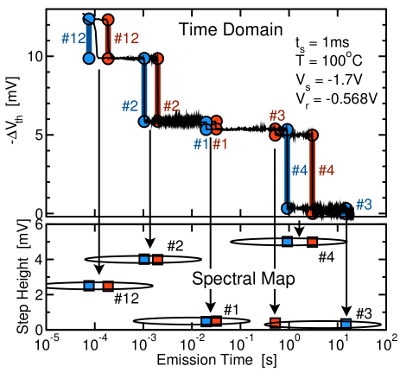
single charging or discharging events [48, 49, 50]. As shown in Fig. 1.1, each of
these events appears as a step in the recovery traces. Interestingly, one can clearly
recognize that those steps differ significantly in their heights. This can be ascribed to
the fact that the random distribution of dopants produces a spatially varying
electrical potential inside the channel. The resulting inhomogeneous current density
from source to drain is frequently referred to as the percolation current path, which is
unique for each device. The lateral position of a charged trap within the gate area
determines the step height in the drain current and the threshold voltage shift.
This height is the signature of each defect and can thus be used for the
identification of a single trap. This fact has motivated the use of the so-called
spectral maps [51, 52, 53], in which the frequency of emission events is plotted
vs.  and
and  (see the lower panel of Fig. 1.1). These maps reveal the
characteristic emission times for certain stress conditions, which can be varied for
the investigation of field and temperature dependence of
(see the lower panel of Fig. 1.1). These maps reveal the
characteristic emission times for certain stress conditions, which can be varied for
the investigation of field and temperature dependence of  and
and  (Fig. 1.2).
TDDS has lead to several essential findings [51, 52, 53, 54] outlined in the
following:
- The plot in Fig. 1.2 reveals that the defects exhibit a strong, nearly
exponential voltage dependence of
 . Empirically, this dependence can
be described by
. Empirically, this dependence can
be described by  . However, it differs from defect to
defect, implying that it is related to certain defect properties.
. However, it differs from defect to
defect, implying that it is related to certain defect properties.
- The time constant plots show a marked temperature dependence, which
becomes obvious by the downward shift of the
 curves for higher
temperatures. The activation energies
curves for higher
temperatures. The activation energies  extracted from Arrhenius
plots are about
extracted from Arrhenius
plots are about  .
.
 of most defects is unaffected by changes in
  (“normal” behavior).
- A few defects show a drop in
 towards lower
  (“anomalous”
behavior).
(“anomalous”
behavior).
- The
 of both types shows a temperature activation with a large spread
(
of both types shows a temperature activation with a large spread
( ).
).
One should keep in mind that some defects exhibit an exponential oxide field
dependence of  in normal random telegraph noise (RTN) measurements [55].
This difference to TDDS findings may arise from the fact that these defects are not
assessable by the TDDS measurements.
in normal random telegraph noise (RTN) measurements [55].
This difference to TDDS findings may arise from the fact that these defects are not
assessable by the TDDS measurements.
Astonishingly, several TDDS recovery traces display RTN only after stressing [51].
The noise at one recovery trace is physically linked to defects — in this case hole
traps — which continuously exchange charge carriers with the substrate. After a
while, the RTN signal vanishes and does not reoccur during the remaining
measurement time. The termination of the noise signal is ascribed to hole traps
which change to their neutral charge state and remain therein. In [51], this kind of
noise has been termed temporary RTN (tRTN) since it occurs only for a limited
amount of time.
A similar phenomenon called anomalous RTN (aRTN) has been discovered in the
early studies of Kirton and Uren [56]. Therein, electron traps have been observed,
which repeatedly produce noise for random time intervals. During the interruptions
of the signal, the defects dwell in their negative charge state so that no noise signal is
generated. The behavior of these traps has been interpreted by the existence of a
metastable defect state.

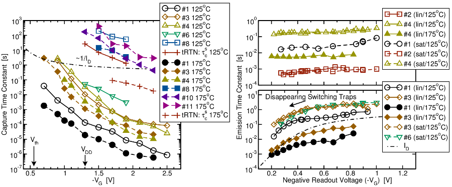
 as a function of
  for
a number of defects at different temperatures extracted from a single device.
Open and closed symbols mark measurements carried out at
for
a number of defects at different temperatures extracted from a single device.
Open and closed symbols mark measurements carried out at  and
and
 , respectively. The
  curves show a strong field acceleration and
temperature activation. However, the observed field acceleration does not follow
the
curves show a strong field acceleration and
temperature activation. However, the observed field acceleration does not follow
the  dependence (dot-dashed line) as predicted by the conventional
SRH model.
dependence (dot-dashed line) as predicted by the conventional
SRH model.  . The two distinct field dependences (upper and lower panel)
suggest the existence of two types of defects present in the oxide. However, the
defect
. The two distinct field dependences (upper and lower panel)
suggest the existence of two types of defects present in the oxide. However, the
defect  shows different field behaviors depending on whether the device is
operated in the linear or the saturation regime during the measurement. This
suggests that the electrostatics within the device are responsible for the two
distinct field dependences. It is noteworthy that the drop in
shows different field behaviors depending on whether the device is
operated in the linear or the saturation regime during the measurement. This
suggests that the electrostatics within the device are responsible for the two
distinct field dependences. It is noteworthy that the drop in  goes hand
in hand with the decrease of the interfacial hole concentration
goes hand
in hand with the decrease of the interfacial hole concentration  (dot-dashed
line).
(dot-dashed
line).