2.1 Tunneling — A Process Depending on Device Electrostatics
Since NBTI is triggered by the electric field  across the dielectric, much
importance is attached to the electrostatics within the device. Since source and drain
are grounded during NBTI stress, the electrical potential remains almost constant
along the interface so that the charge carriers face the same conditions for charge
trapping over the entire channel area. As a consequence, the description of this
process can be reduced to a one-dimensional problem (in the
across the dielectric, much
importance is attached to the electrostatics within the device. Since source and drain
are grounded during NBTI stress, the electrical potential remains almost constant
along the interface so that the charge carriers face the same conditions for charge
trapping over the entire channel area. As a consequence, the description of this
process can be reduced to a one-dimensional problem (in the  -direction) where the
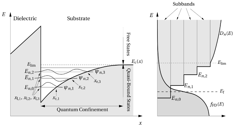
electrostatics are only governed by the gate bias. The corresponding band diagram of
a MOSFET with a p-doped silicon substrate biased in inversion is depicted in
Fig. 2.1 (left). Due to the potential difference between substrate and gate, the
band edges are strongly bent close to the interface so that the conduction
band
-direction) where the
electrostatics are only governed by the gate bias. The corresponding band diagram of
a MOSFET with a p-doped silicon substrate biased in inversion is depicted in
Fig. 2.1 (left). Due to the potential difference between substrate and gate, the
band edges are strongly bent close to the interface so that the conduction
band  forms a potential well. The electrons therein are confined to a
small region close to the interface, which results in the build-up of discrete
quasi-bound states
forms a potential well. The electrons therein are confined to a
small region close to the interface, which results in the build-up of discrete
quasi-bound states  ,
,  ,
,  ,
,  as shown in Fig. 2.1. The energetical
separation between these states narrows towards higher energies and changes to a
continuum of free states at the energy
as shown in Fig. 2.1. The energetical
separation between these states narrows towards higher energies and changes to a
continuum of free states at the energy  . In the two other dimensions
(
. In the two other dimensions
( -plane), the channel electrons behave as free particles and can therefore
carry a current in these directions. The combination of quasi-bound and free
states yields subbands as illustrated in Fig. 2.1 (right). Therefore, steps
appear in the electron density of states (DOS)
-plane), the channel electrons behave as free particles and can therefore
carry a current in these directions. The combination of quasi-bound and free
states yields subbands as illustrated in Fig. 2.1 (right). Therefore, steps
appear in the electron density of states (DOS)  , where each step
belongs to one subband. The occupation probability of a state is given by
Fermi-Dirac statistics, which apply as long as thermal equilibrium prevails. This is
certainly the case for NBTI conditions, where the channel does not carry
any appreciable current. Indeed, small and short channel current pulses,
required in some measurement techniques to assess the NBTI degradation, lead
to an overpopulation of high energy states. However, at the end of each
pulse, the redistribution of the charge carriers back to equilibrium proceeds
quickly and thus has not been noticed in experiments up to now. For this
reason, electrons are assumed to obey the Fermi-Dirac statistics during NBTI
conditions.
, where each step
belongs to one subband. The occupation probability of a state is given by
Fermi-Dirac statistics, which apply as long as thermal equilibrium prevails. This is
certainly the case for NBTI conditions, where the channel does not carry
any appreciable current. Indeed, small and short channel current pulses,
required in some measurement techniques to assess the NBTI degradation, lead
to an overpopulation of high energy states. However, at the end of each
pulse, the redistribution of the charge carriers back to equilibrium proceeds
quickly and thus has not been noticed in experiments up to now. For this
reason, electrons are assumed to obey the Fermi-Dirac statistics during NBTI
conditions.
There exist several approximate methods to obtain the wavefunctions of bound
states, however, each of them suffers from oversimplifications in certain regions. The
first approach makes use of the Airy functions [98], which are solutions of the
Schrödinger equation when the inversion layer is approximated by triangular
potential well. Even though these functions satisfactorily reproduce the oscillatory
behavior within the channel, they lack the exponential tails penetrating into the
dielectric. This is due to the fact that the discontinuity at the interface is
approximated by an infinitely high barrier. Another approach is provided by
Gundlach’s method [99] that focuses on the part of the wavefunctions located within
the dielectric. The channel electrons, however, are modeled as free particles in a
constant potential and thus the effect of the electric field within the channel is
not considered in this method. The third analytical approach relies on the
Wentzel-Kramers-Brillouin (WKB) approximation [100, 101] (see Appendix A.2),
which stems from a semi-classical derivation. However, this approximation
breaks down at the classical turning points  ,
,  ,
, 
 where
the energies of the quasi-bound states
where
the energies of the quasi-bound states  ,
,  ,
,  ,
, fall below
the conduction band edge
fall below
the conduction band edge  . This problem can be overcome using
Langer’s method [102], which yields reasonable results — even in a region
close to the classical turning points — and is thus frequently applied for
the calculation of the tunneling probability. The most interesting part of
the wavefunctions lies in the region left to the interface where the WKB
approximation is often simplified assuming a trapezoidal, a triangular, or even a
rectangular energy barrier (see Appendix A.3). The above deficiencies can be
overcome by numerically solving the Schrödinger equation for the whole region
including the substrate and the dielectric. This, for instance, is carried out in a
Schrödinger-Poisson solver, which also considers the electrostatics within the device
(see Chapter 3).
. This problem can be overcome using
Langer’s method [102], which yields reasonable results — even in a region
close to the classical turning points — and is thus frequently applied for
the calculation of the tunneling probability. The most interesting part of
the wavefunctions lies in the region left to the interface where the WKB
approximation is often simplified assuming a trapezoidal, a triangular, or even a
rectangular energy barrier (see Appendix A.3). The above deficiencies can be
overcome by numerically solving the Schrödinger equation for the whole region
including the substrate and the dielectric. This, for instance, is carried out in a
Schrödinger-Poisson solver, which also considers the electrostatics within the device
(see Chapter 3).
The injection of electrons into the dielectric is hindered in crystal and amorphous
structures due to the absence of any quantum states within their bandgap. Atomic
arrangements, where the symmetry of the regular structure is broken, are termed
defects. During processing they unavoidably arise in large abundance and are
distributed over the whole oxide. Furthermore, these defects have orbitals that can
potentially introduce energy levels within the insulator bandgap and are thus capable
of capturing and emitting substrate charge carriers. The band edges of the dielectric
are large energy barriers for the charge carriers in the substrate. Since the band
offset between the substrate and the dielectric has values of several electron
volts, thermal activation over these barriers is negligible when there is only a
small bias applied between source and drain. However, the wavefunctions
of the charge carriers feature quickly decaying tails into the oxide. This
implies a non-zero probability of encountering charge carriers within the
dielectric, meaning that they penetrate into the dielectric and can be captured
by defects. The rates of such transitions are given by Fermi’s golden rule.

The subscripts  and
and  denote the initial and the final state of the tunneling
electron.
denote the initial and the final state of the tunneling
electron.  is a matrix element, which is associated with the transition and can
be calculated as
is a matrix element, which is associated with the transition and can
be calculated as

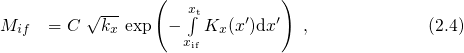
The term  in equation (2.1) guarantees energy conservation
before and after the transition. This kind of process is commonly referred
to as ‘elastic’, where this term only refers to the energy of the exchanged
electron.
in equation (2.1) guarantees energy conservation
before and after the transition. This kind of process is commonly referred
to as ‘elastic’, where this term only refers to the energy of the exchanged
electron.
Tewksbury [23] provided an expression for matrix element assuming a constant oxide
field within the dielectric and a constant potential within the substrate. In his
derivation, the trap was approximated by a  -type potential
with  being the Dirac delta function.
  and
and  are the conduction
band edge in the oxide and the depth of the trap potential, respectively. The form of
this potential implies that the integral in the matrix element only contributes
directly at the center of the trap. Then the matrix element has the form
where
are the conduction
band edge in the oxide and the depth of the trap potential, respectively. The form of
this potential implies that the integral in the matrix element only contributes
directly at the center of the trap. Then the matrix element has the form
where  and
and  are defined as the wavevectors within the substrate and the
dielectric, respectively.
are defined as the wavevectors within the substrate and the
dielectric, respectively.  denotes the energy of the electrons in the
  -direction and
  is a
normalization constant.
is a
normalization constant.  stands for the spatial depth of a trap measured from the
substrate-oxide interface and
stands for the spatial depth of a trap measured from the
substrate-oxide interface and  is the position of the interface.
  represents the
tunneling mass and
represents the
tunneling mass and  is the electron mass in the conduction band. Note that the
exponential term in equation (2.4) is the dominant factor in the matrix element. For
slowly varying
is the electron mass in the conduction band. Note that the
exponential term in equation (2.4) is the dominant factor in the matrix element. For
slowly varying  , it decays with increasing trap depth — a behavior
characteristic for all kinds of tunneling processes. The WKB integral in its
exponent originates from the phase factor of the channel wavefunction, whose
corresponding wavevector
, it decays with increasing trap depth — a behavior
characteristic for all kinds of tunneling processes. The WKB integral in its
exponent originates from the phase factor of the channel wavefunction, whose
corresponding wavevector  is often approximated to be constant for
simplicity [23]. Due to the reduction to a one-dimensional problem, the
is often approximated to be constant for
simplicity [23]. Due to the reduction to a one-dimensional problem, the  -type trap
potential covers the entire plane parallel to the interface. To correct for this
shortcoming, Tewksbury introduced a capture cross section following the Freeman
approach [103].
-type trap
potential covers the entire plane parallel to the interface. To correct for this
shortcoming, Tewksbury introduced a capture cross section following the Freeman
approach [103].
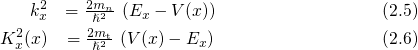
Lundstrom et al. [104] derived an expression of the matrix element assuming a
step-potential for  and a three-dimensional
  -type trap potential [104].
 stands for the height of the potential step. The wavevectors parallel to the
interface are referred to as
stands for the height of the potential step. The wavevectors parallel to the
interface are referred to as  and
and  . Due to the constant potential energy within
the dielectric, the WKB integrand is reduced to a simple multiplication
. Due to the constant potential energy within
the dielectric, the WKB integrand is reduced to a simple multiplication
 . Keep in mind that the kinetic energy of the electrons perpendicular to
the interface enters the exponential term in contrast to equation (2.4). The sum of
this matrix element over all conduction band states assuming a free Fermi gas
delivers a tunneling time constant of the form where the prefactor
. Keep in mind that the kinetic energy of the electrons perpendicular to
the interface enters the exponential term in contrast to equation (2.4). The sum of
this matrix element over all conduction band states assuming a free Fermi gas
delivers a tunneling time constant of the form where the prefactor  is shown to weakly depend on the trap energy
  and
the trap depth
and
the trap depth  . Note that wavevector
  , the equivalent quantity to
  in the
one-dimensional case, enters the exponential term again.
in the
one-dimensional case, enters the exponential term again.
The mechanism of pure elastic electron tunneling is often used as the standard
explanation of charge trapping in MOSFETs. Over the time, several simplified
expressions of tunneling rates have been published in numerous distinct charge
trapping models [105, 106] and will be touched on for completeness below.
Christenson et al. [106] used Shockley-Read-Hall statistics in order to investigate
the low frequency noise spectrum of a MOS transistor. His hole capture rates
incorporate a tunneling probability through a rectangular potential barrier depending
on the depth of a trap  .
.
where  and
and  stand for a capture coefficient and the barrier height, respectively.
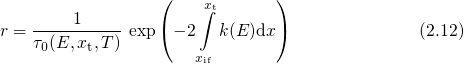
A further improvement has been achieved by Scharf [97], who accounted for the
energy dependence of the tunneling charge carriers. Here, the integral extends from the semiconductor-oxide interface
stand for a capture coefficient and the barrier height, respectively.
A further improvement has been achieved by Scharf [97], who accounted for the
energy dependence of the tunneling charge carriers. Here, the integral extends from the semiconductor-oxide interface  to trap depth
 . Note that the second factor on the right-hand side of equation (2.12)
corresponds to a WKB factor and reflects the exponentially decaying tunneling
probability with increasing trap depth. However, this factor has been
phenomenologically introduced by Scharf but does not arise from a rigorous
derivation. The approximation provided by Tewksbury is the most suited
one for the application to MOSFETs since it accounts for the energy and
depth dependence and uses a convenient one-dimensional formulation of
tunneling.
. Note that the second factor on the right-hand side of equation (2.12)
corresponds to a WKB factor and reflects the exponentially decaying tunneling
probability with increasing trap depth. However, this factor has been
phenomenologically introduced by Scharf but does not arise from a rigorous
derivation. The approximation provided by Tewksbury is the most suited
one for the application to MOSFETs since it accounts for the energy and
depth dependence and uses a convenient one-dimensional formulation of
tunneling.
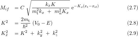
 ,
,  ,
,  ,
,  are spatially
confined between the dielectric on the left-hand side and the conduction band
on the right-hand side. The free states encounter no boundary on the right-hand
side and are energetically located above the quasi-bound states
are spatially
confined between the dielectric on the left-hand side and the conduction band
on the right-hand side. The free states encounter no boundary on the right-hand
side and are energetically located above the quasi-bound states  ,
,  ,
,
 ,
,  at the conduction band edge deep in the substrate (
 ).
).  and the Fermi-Dirac distribution
  . Each
quasi-bound state associated with its own subband, resulting in a stepped DOS.
The Fermi energy
. Each
quasi-bound state associated with its own subband, resulting in a stepped DOS.
The Fermi energy  places the Fermi-Dirac distribution relative to the DOS
and determines the occupation of each state.
places the Fermi-Dirac distribution relative to the DOS
and determines the occupation of each state.