


Next: 6.3 Examples
Up: 6.2 Circuit Equation Damping
Previous: 6.2.4 Local Limiting
6.2.5 The New Method
Damping of the contact voltages in general-purpose device simulation is
different in two aspects. Firstly, arbitrary devices with arbitrary
characteristics and an arbitrary number of nodes can be simulated.
Secondly, for compact models only potential differences are used (
V =  -
-  ) whereas the contact models in device simulation
normally use absolute potential values. This implies that a DC offset
which does not change anything about the solution will waste
computation time as it needs many iterations to build up the proper potential
distribution inside the device. This is due to the fact, that the potential
is initialized to the so-called built-in potential which evaluates to [15]
) whereas the contact models in device simulation
normally use absolute potential values. This implies that a DC offset
which does not change anything about the solution will waste
computation time as it needs many iterations to build up the proper potential
distribution inside the device. This is due to the fact, that the potential
is initialized to the so-called built-in potential which evaluates to [15]
 |
=  + VT . ln
  . .  NT + NT + 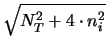

 |
NT > 0 |
|
| |
=  - VT . ln
  . .  - NT +

 |
NT < 0 |
(6.9) |
with NT being the net dopant concentration. For NT > 0 the first
version and for NT < 0 the second version of (6.9)
should be used to avoid cancellation errors for large absolute values of NT.
(6.9) is an excellent guess for the potential
in non-depletion regions when all contact voltages are zero. However, this
initial-guess could be improved by adding the average of the contact voltages.
Unfortunately this cannot be done for a mixed-mode simulation as the contact
voltages evolve during iteration and hence are not known in advance.
To make use of the damping strategy (6.8) device
nodes were grouped in pairs using available information about the device
(diode, bipolar junction transistor or MOS transistor). Then the contact
voltages were damped using (6.8). However, the
solution of the semiconductor equations is damped using a global damping
strategy
with a global damping factor d which applies to all solution
variables in the same way. An important feature of
(6.10) is that the direction of the update does not
change which is not the case when applying
(6.8). In experiments it was tried to limit the
node voltages using (6.8) whereas for the rest
of the solution vector (6.10) was applied. As the
node voltages are directly coupled to the contact voltages by
(5.27) and the contact voltages determine the potential inside
the device this caused inconsistencies which lead to strong oscillations of
the solution variables. Hence, further investigations of this mixed damping
procedure were skipped.
A circuit revealing the problems caused by DC offsets is shown in
Fig. 6.2. Here
V1 = VD + VDC and
V2 = VDC with
VD = 1 V. First, the circuit is
simulated using the direct boundary condition (DBC) given in
(5.27). The evolution of the node voltages and the device
contact voltages during iteration for
VDC = 0 V is
shown in Fig. 6.3. Until convergence 10 iterations
are needed. However, when setting
VDC = 10 V
convergence properties deteriorate (35 iterations) as shown in
Fig. 6.4 since it takes many iterations to build up the
high potential inside the diode. As for the device operation only potential
differences are relevant, a modified boundary condition can be formulated.
Using one of the device terminal voltages as reference voltage the boundary
condition (5.27) can be reformulated to yield
for a general node and
f = =  = 0
= 0 |
(6.12) |
for the reference node. The MNA stamp for a general node reads
| jx, y |
|
 |
 |
IC |
r |
|
|
|
|
|
-1 |
f k k |
|
1 |
-1 |
-1 |
|
f k k |
| IC |
|
|
|
-1 |
fICk |
whereas it simplifies to
| jx, y |
|
IC |
r |
|
|
|
-1 |
fk |
|
1 |
|
|
| IC |
|
-1 |
fICk |
Figure 6.2:
Problematic constellation when using DBC.
![\begin{figure}
\begin{center}
\resizebox{7.8cm}{!}{
\psfrag{I}{$\scriptstyle I$}...
...ludegraphics[width=7.8cm,angle=0]{figures/diode-dc.eps}}\end{center}\end{figure}](img481.gif) |
Figure 6.3:
Evolution of the node and contact voltages during iteration using DBC
with no DC component. Until convergence 10 iterations are needed.
![\begin{figure}
\begin{center}
\resizebox{11.4cm}{!}{
\psfrag{0} [r][r]{$\textsty...
...egraphics[width=11.4cm,angle=0]{figures/diode-dc_0.eps}}\end{center}\end{figure}](img482.gif) |
Figure 6.4:
Evolution of the node and contact voltages during iteration using DBC
with DC component. Until convergence 35 iterations are needed.
![\begin{figure}
\begin{center}
\resizebox{11.4cm}{!}{
\psfrag{-2} [r][r]{$\textst...
...graphics[width=11.4cm,angle=0]{figures/diode-dc_10.eps}}\end{center}\end{figure}](img483.gif) |
Figure 6.5:
Evolution of the node and contact voltages during iteration using RBC
with DC component. As for no DC component, 10 iterations are needed
until convergence.
![\begin{figure}
\begin{center}
\resizebox{11.4cm}{!}{
\psfrag{-2} [r][r]{$\textst...
...ics[width=11.4cm,angle=0]{figures/diode-dc_refnode.eps}}\end{center}\end{figure}](img484.gif) |
Figure 6.6:
Effect of global and local damping on the solution variables: a) global damping b) local damping.
![\begin{figure}
\begin{center}
\resizebox{16cm}{!}{
\psfrag{a} {$\scriptstyle a)$...
...udegraphics[width=16cm,angle=0]{figures/local-damp.eps}}\end{center}\end{figure}](img485.gif) |
for the reference node. The simulation results using this reference
boundary condition (RBC) are shown in Fig. 6.5.
As for
VDC = 0 V, 10 iterations are needed until
convergence. However, an imminent problem of this approach is that the
boundary condition obtained for the reference node shows no dependence on the
node voltage
. This means that when fIC is
pre-eliminated the main-diagonal will be zero for
f
resulting in a singular equation system if the contact node is not connected
to other devices providing main-diagonal entries. In addition, the choice of
reference node is crucial and depends on the current operating condition of
the device. It was found to be more useful to take the average of the node
voltages
as reference voltage with nC being the number of contact nodes. This
type of boundary condition will be refered to as average boundary
condition (ABC).
The MNA stamp for a general node reads
| jx, y |
|
 |
|
IC |
r |
|
|
|
|
|
-1 |
fk |
|
1 |
-1 |
-1 |
|
fk |
|
|
-  |
|
|
|
f k k |
| IC |
|
|
|
-1 |
fICk |
It is to note that the row
f is entered for each
contact node, hence one obtains
 = 1. The
convergence properties using ABC for the diode circuit
Fig. 6.2 are similar to RBC as shown in
Fig. 6.5. However, as
= 0.5 V
the internal contact voltages are
= 1. The
convergence properties using ABC for the diode circuit
Fig. 6.2 are similar to RBC as shown in
Fig. 6.5. However, as
= 0.5 V
the internal contact voltages are
 0.5 V the built-in potential
provides a better initial-guess and only 7 iterations are needed.
0.5 V the built-in potential
provides a better initial-guess and only 7 iterations are needed.
Figure 6.7:
Placement of the iteration dependent conductance GSk for one terminal.
![\begin{figure}
\begin{center}
\resizebox{7.8cm}{!}{
\psfrag{IB}{$\scriptstyle I_...
...degraphics[width=7.8cm,angle=0]{figures/av-contact.eps}}\end{center}\end{figure}](img490.gif) |
It has been observed that the full coupled system of device and circuit
equations is extremely instable at the beginning of the iteration. Similar
observations were made by Ho et al. [32] for FET circuits using compact
models. They proposed to shunt a resistor of
3 k at the
source and drain during the first three Newton iterations,
to stabilize the coupled system and to slightly decouple the device from the
circuit equations. This approach has been extended by introducing an iteration
dependent conductance GSk between each device node and ground
as shown in Fig. 6.7.
The following purely empirical expression for GSk delivered very promising results
at the
source and drain during the first three Newton iterations,
to stabilize the coupled system and to slightly decouple the device from the
circuit equations. This approach has been extended by introducing an iteration
dependent conductance GSk between each device node and ground
as shown in Fig. 6.7.
The following purely empirical expression for GSk delivered very promising results
| G0 |
= |
10-2 S |
(6.14) |
| Gmin |
= |
10-12 S |
(6.15) |
| GSk |
= |
 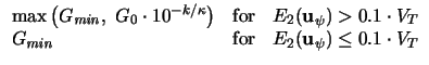
 |
(6.16) |
 |
= |
1.0 ... 4.0 |
(6.17) |
with k being the iteration counter. It is worthwhile to note that the
algorithm worked equally well with
Gmin = 0 for the simulated
circuits. However, this expression is purely empirical but unfortunately any
attempt to use a more rigorous expression based on norms of the quantities did
not work satisfactory.
Next: 6.3 Examples
Up: 6.2 Circuit Equation Damping
Previous: 6.2.4 Local Limiting
Tibor Grasser
1999-05-31