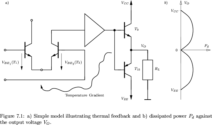
Thermal effects are of fundamental importance for the chip design of integrated circuits. Typical operational amplifiers (OpAmps) can deliver powers of 50-100 mW to a load, and as the output stage internally dissipates similar power levels the temperature of the chip rises in proportion to the dissipated output power [45,64]. As the transistors are very densely packed, self-heating of the output stage will affect all other transistors. This is especially true as silicon is a good thermal conductor, so the whole chip tends to rise to the same temperature as the output stage. However, small temperature gradients develop across the chip with the output stage being the heat source. The temperature coefficient of the junction voltage for forward-biased pn-junctions is known to be approximately -2 mV/K, that is to obtain the same current a smaller junction voltage is needed. As shown in Fig. 7.25 these temperature gradients appear across the input components of the OpAmp and induce an additional input voltage difference which is proportional to the output dissipated power.
![\begin{figure}
\begin{center}
\resizebox{16cm}{!}{
\psfrag{T1} {$\scriptstyle T_...
...includegraphics[width=16cm,angle=0]{figures/layout.eps}}\end{center}\end{figure}](img565.gif) |
To give an approximate expression for this effect, it can be assumed, to a first order, that the temperature difference T2 - T1 across a pair of matched and closely spaced components is given simply by
The dissipated power in the output stage of Fig. 7.25a can be written as
| Pd = (VS - VO) . IL = |
(7.20) |
| VS = VCC *1cmwhen *0.3cmVO > 0 | (7.21) | ||
| VS = VEE *1cmwhen *0.3cmVO < 0 | (7.22) |
The complete ![]() A709 [59,25] as shown in Fig. 7.27 has
been simulated considering thermal interaction between the input and the
output stage. This circuit is of special interest as it is one of the
SPICE benchmark circuits given in [43]. The DC transfer
characteristic has been calculated with and without thermal interaction.
Consideration of thermal interaction was done by solving the lattice heat flow
equation for the transistors T1, T2, T9 and T15 and by
assuming a thermal network as shown in Fig. 7.28. The
thermal conductances were assumed to be
G1 = G2 = 2 mW/K and
G9 = G15 = 10 mW/K while the coupling mismatch was modeled by
G1, 9 = G1, 15 = Gk = 10 mW/K and
G2, 9 = G2, 15 = Gk . (1 -
A709 [59,25] as shown in Fig. 7.27 has
been simulated considering thermal interaction between the input and the
output stage. This circuit is of special interest as it is one of the
SPICE benchmark circuits given in [43]. The DC transfer
characteristic has been calculated with and without thermal interaction.
Consideration of thermal interaction was done by solving the lattice heat flow
equation for the transistors T1, T2, T9 and T15 and by
assuming a thermal network as shown in Fig. 7.28. The
thermal conductances were assumed to be
G1 = G2 = 2 mW/K and
G9 = G15 = 10 mW/K while the coupling mismatch was modeled by
G1, 9 = G1, 15 = Gk = 10 mW/K and
G2, 9 = G2, 15 = Gk . (1 - ![]() ) with
) with ![]() being the mismatch parameter which is
proportional to the temperature gradient across the input transistors
[45].
being the mismatch parameter which is
proportional to the temperature gradient across the input transistors
[45].
The solution of the fully coupled equation system is possible with a proper
iteration scheme. A small change in the output voltage during iteration
causes a large change in the collector current of the conducting output
transistor. The dissipated power changes and with it the temperature
distribution inside the output transistor. This modified power alters the
base-emitter voltages of the input transistors which produces a change in the
base-emitter voltages of the output transistors. As all these coupling
mechanisms are highly non-linear special precautions have to be taken. The
iteration scheme given in Section 7.4 could be used. However, as the
simulation failed very frequently for too large steps of the input voltage an
additional failure criterion in the Thermal block was added. When
the step of the input voltage was too large it caused oscillations in the
solution which, due to the strong non-linearities, blew up the lattice
temperatures. This took approximately 30 iterations which were very
expensive in computational terms as each iteration took approximately 20
-200 seconds depending on the condition of the system matrix. So this
event had to be detected as soon as possible. It was found that an abnormal
behavior of the potential update norm
E![]() (u
(u![]() ) was a good
indication of starting oscillations. Hence, whenever
E
) was a good
indication of starting oscillations. Hence, whenever
E![]() (u
(u![]() ) was larger than approximately
102 . VT
after 10 iterations or whenever
E
) was larger than approximately
102 . VT
after 10 iterations or whenever
E![]() (u
(u![]() ) exceeded
105 . VT the iteration was canceled. Furthermore, the number of
iterations was limited to 30.
) exceeded
105 . VT the iteration was canceled. Furthermore, the number of
iterations was limited to 30.
An additional, even worse, phenomenon was observed when solving the fully
coupled system in the Thermal block. Even for
E![]() (u) already as small as 10-2 the iterative solver
failed and also generated a failure event.
(u) already as small as 10-2 the iterative solver
failed and also generated a failure event.
These failure events were handled by reducing the increment of the input voltage by a factor of 2. Whenever the system could again be solved within 15 iterations the step size was doubled until the original step size was obtained.
The iteration scheme was inherited from ThermalDD as given in Section 7.4 with an unmodified Electric block. The ThermalPre and the Thermal block were augmented by the failure criterion given above
ThermalDD_2 : ThermalDD
{
   aux f = !firstStep &&
              ((updateNormPot > 1e5) ||
                  (iterationCount > 10 && updateNormPot > 1e3) ||
                  (iterationCount > 30));

   ThermalPre
   {
      failure = ^f;
   }
   Thermal
   {
      failure = ^f;
   }
}
The DC transfer characteristic was calculated by stepping
![]() from -1 mV to 1 mV with
from -1 mV to 1 mV with
![]()
![]() = 20
= 20 ![]() V. From SPICE simulations the
open-loop gain of the
V. From SPICE simulations the
open-loop gain of the ![]() A709 was known to be approximately 35000 so for each
step of
A709 was known to be approximately 35000 so for each
step of
![]()
![]() a step of 0.7 V could be
expected for
a step of 0.7 V could be
expected for
![]()
![]() which is quite large. However,
no convergence problems occurred until
which is quite large. However,
no convergence problems occurred until
![]() approached 0 V.
This was the most critical part of the simulation and several step reductions
were necessary for both the pure electrical and the thermal simulation.
The size of the system matrix was 37177 and 40449 for constant temperature
and thermal simulation, respectively, and the simulation took 9 and 25
hours on a Linux Pentium II 350MHz workstation. For the thermal simulation
the conditioning of the system matrix was found to be very poor and
several step reductions were necessary.
approached 0 V.
This was the most critical part of the simulation and several step reductions
were necessary for both the pure electrical and the thermal simulation.
The size of the system matrix was 37177 and 40449 for constant temperature
and thermal simulation, respectively, and the simulation took 9 and 25
hours on a Linux Pentium II 350MHz workstation. For the thermal simulation
the conditioning of the system matrix was found to be very poor and
several step reductions were necessary.
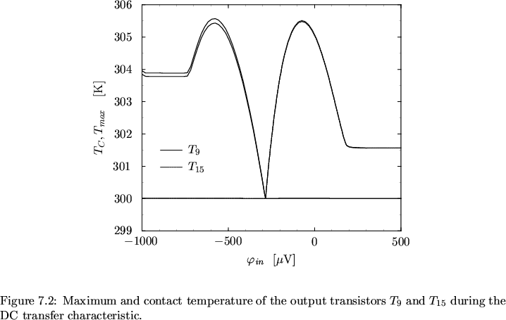
The DC transfer characteristic is shown in Fig. 7.29 with the obvious humps resulting from thermal feedback effects. In Fig. 7.30 the open-loop voltage gain Av is shown and the dramatic impact of thermal coupling. The thermal conductances assumed in this simulation were very optimistic and an even stronger impact of thermal coupling has been published in literature [38,18]. For stronger coupling, even the sign of the open-loop voltage gain may change and cause the OpAmp to become unstable.
The maximum temperature and the contact temperature of the output stage are
shown in Fig. 7.31. It is obvious that the self-heating
inside the transistor plays only a minor role at these current levels.
However, the power dissipated inside the device heats up the NPN transistor
due to the resistive thermal boundary condition which obstruct the heat flow
out of the transistor. This is in accordance to the commonly used assumption
that the transistor can be modeled by a power source alone
(cf. Appendix A). The PNP transistor has only a ![]() of
approximately 10 and comparable current levels have been obtained by
increasing the emitter area of the transistor
(
WPNP/WNPN = 5). Hence the locally generated heat
density H is even smaller than for the NPN transistor and the temperature
drop inside the device is negligible.
of
approximately 10 and comparable current levels have been obtained by
increasing the emitter area of the transistor
(
WPNP/WNPN = 5). Hence the locally generated heat
density H is even smaller than for the NPN transistor and the temperature
drop inside the device is negligible.
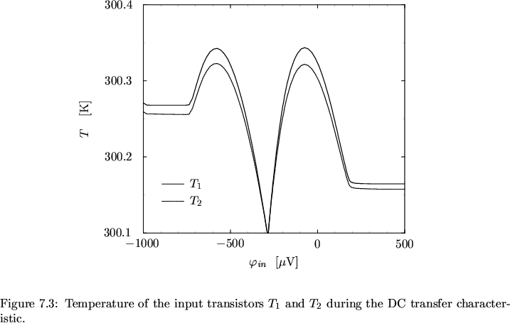
A similar situation occurs for input transistors T1 and T2.
As they are biased with
IC = 20 ![]() A only self-heating
is negligible and the contact temperature resembles the heat transfered
from the output stage. As unsymmetric thermal conductivities have
been assumed the temperature of T1 is always slightly higher than the
temperature of T2. The temperature difference
T2 - T1 is shown
in Fig. 7.33 with a maximum of only -22 mK.
Even this small temperature difference has a strong impact on the output
characteristic due to the high gain of the circuit.
A only self-heating
is negligible and the contact temperature resembles the heat transfered
from the output stage. As unsymmetric thermal conductivities have
been assumed the temperature of T1 is always slightly higher than the
temperature of T2. The temperature difference
T2 - T1 is shown
in Fig. 7.33 with a maximum of only -22 mK.
Even this small temperature difference has a strong impact on the output
characteristic due to the high gain of the circuit.
![\begin{figure}
\begin{center}
\resizebox{11.4cm}{!}{
\psfrag{709_dc_SH_split1.cr...
...egraphics[width=11.4cm,angle=0]{figures/709_dc_n18.eps}}\end{center}\end{figure}](img573.gif) |
![\begin{figure}
\begin{center}
\resizebox{11.4cm}{!}{
\psfrag{709_dc_SH_split1.cr...
...udegraphics[width=11.4cm,angle=0]{figures/709_gain.eps}}\end{center}\end{figure}](img574.gif) |
![\begin{figure}
\begin{center}
\resizebox{11.4cm}{!}{
\psfrag{709_dc_SH_split2.cr...
...degraphics[width=11.4cm,angle=0]{figures/709_dc_dT.eps}}\end{center}\end{figure}](img577.gif) |
![\begin{figure}
\begin{center}
\resizebox{16cm}{!}{
\psfrag{Vin} {$\scriptstyle \...
...\includegraphics[width=16cm,angle=0]{figures/ua709.eps}}\end{center}\end{figure}](img572.gif)
![\begin{figure}
\begin{center}
\resizebox{16cm}{!}{
\psfrag{TREF}{$\scriptstyle \...
...cludegraphics[width=16cm,angle=0]{figures/dp-therm.eps}}\end{center}\end{figure}](img559.gif)
![\begin{figure}
\begin{center}
\resizebox{11.4cm}{!}{
\psfrag{709_dc_SH_P.crv:P} ...
...udegraphics[width=11.4cm,angle=0]{figures/709_dc_P.eps}}\end{center}\end{figure}](img578.gif)