The dashed curve and the data  and
and  are connected with
the second problem. In order to obtain the exact solution to this problem,
a procedure similar to that performed for solving the first problem may be
employed. This is not only cumbersome, but also not necessary. Hence, an
approximate, but very simple solution to the second problem is developed,
which relies on the solution to the first problem. Let us assume that the width
of the depletion region in the bulk is
are connected with
the second problem. In order to obtain the exact solution to this problem,
a procedure similar to that performed for solving the first problem may be
employed. This is not only cumbersome, but also not necessary. Hence, an
approximate, but very simple solution to the second problem is developed,
which relies on the solution to the first problem. Let us assume that the width
of the depletion region in the bulk is  for the gate bias
  .
No interface charge is present in device at the moment. Suppose that the gate
bias changes to a value
.
No interface charge is present in device at the moment. Suppose that the gate
bias changes to a value  . For small bias changes
the boundary of the depletion region modulates only slightly
. For small bias changes
the boundary of the depletion region modulates only slightly
 ; the capacitance of the depletion
region
; the capacitance of the depletion
region  remains nearly constant. Under these
conditions the surface potential variation may be found by
remains nearly constant. Under these
conditions the surface potential variation may be found by
Let us insert a localized interface charge into the device. The charge perturb
the surface potential by  which is the solution to the first
problem when
which is the solution to the first
problem when  and
and  are assumed to be constant. The solution
to the second problem follows from the principle of superposition
are assumed to be constant. The solution
to the second problem follows from the principle of superposition :
:
 . This equality means that
  is the
same at the gate bias with the presence of the interface charge as
those at the gate bias and absence of any charge. A connection between
the solutions to both problems can be easily established
is the
same at the gate bias with the presence of the interface charge as
those at the gate bias and absence of any charge. A connection between
the solutions to both problems can be easily established
Remark that  holds. In typical
conditions
holds. In typical
conditions  holds and both solutions come close to each other. In
order to confirm relationship F.21, we have to find an efficient
way to calculate when
holds and both solutions come close to each other. In
order to confirm relationship F.21, we have to find an efficient
way to calculate when  . This case is of interest
because
. This case is of interest
because  becomes comparable to
  . In the absence of a model which
is more convenient than F.15, we will confirm
relationship F.21 for a large width of the depletion region, where
for relationship F.16 is used. As can be seen in
Figure F.2, the theory agrees with the numerical results
(dashed curve versus points).
. In the absence of a model which
is more convenient than F.15, we will confirm
relationship F.21 for a large width of the depletion region, where
for relationship F.16 is used. As can be seen in
Figure F.2, the theory agrees with the numerical results
(dashed curve versus points).
When considering an infinitely long interface charge-sheet,
expression F.21 together with F.17 reduces properly
to the well known result:  . This result is correct
for arbitrary large charge densities, in spite of formula F.21
being derived for small bias changes. For a spatially uniform charge, the same
conditions at the interface automatically result in the same
. This result is correct
for arbitrary large charge densities, in spite of formula F.21
being derived for small bias changes. For a spatially uniform charge, the same
conditions at the interface automatically result in the same  and
expression F.21 still remains valid.
and
expression F.21 still remains valid.
As derived, the extreme value of the band-bending is
 , whereas for the gate-bias shift
 . From F.17 it follows
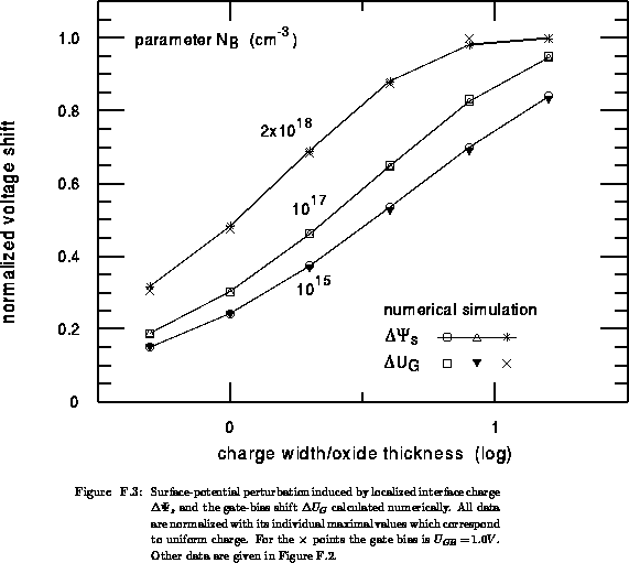
To confirm this equality we plotted the numerical data from
Figure F.2 normalized with the extreme values
(Figure F.3). The extremes are calculated by numerical simulation,
assuming uniform charge along the whole channel. Additional calculations are
performed for heavily doped bulk  , depleted
shallowly so that
, depleted
shallowly so that  . These results are depicted by the
points
. These results are depicted by the
points  and
and  . Numerical simulations nicely reflect
relationship F.22. Small differences between the normalized
. Numerical simulations nicely reflect
relationship F.22. Small differences between the normalized
 and
and  data for the same bulk dopant concentration
originate due to different (just under the traps) in the calculations. In
the main text, Section 3.5, we have adduced that the field
lines from the interface surrounding the charge end in the space-charge region
under the localized charge. Is has been heuristically concluded that this
two-dimensional effect reduces the perturbation of the surface potential. This
conclusion is not in coherence with Figure F.2, where
for a finite falls below the characteristic for an infinite
, because we expect that the two-dimensional effect attenuates with
decreasing . However, the lowering of with stems from
lowering the extreme
data for the same bulk dopant concentration
originate due to different (just under the traps) in the calculations. In
the main text, Section 3.5, we have adduced that the field
lines from the interface surrounding the charge end in the space-charge region
under the localized charge. Is has been heuristically concluded that this
two-dimensional effect reduces the perturbation of the surface potential. This
conclusion is not in coherence with Figure F.2, where
for a finite falls below the characteristic for an infinite
, because we expect that the two-dimensional effect attenuates with
decreasing . However, the lowering of with stems from
lowering the extreme  , while the ratio
 increases as a consequence of the reduced
two-dimensional effect. With decreasing , the factor
increases as a consequence of the reduced
two-dimensional effect. With decreasing , the factor  increases. It turns out that increases with decreasing ,
approaching the value which corresponds to the uniform charge.
increases. It turns out that increases with decreasing ,
approaching the value which corresponds to the uniform charge.
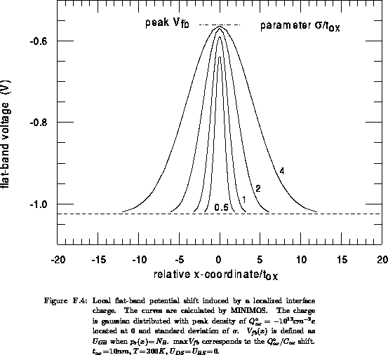
Figure F.4 shows the spatial distribution of the flat-band
potential in our long channel MOSFET in the presence of interface charge,
computed numerically. The bulk is uniform, heavily doped
 , of
, of  -type. The local flat-band potential
 is defined as the gate-bulk voltage which induces the flat-band
condition at the point
is defined as the gate-bulk voltage which induces the flat-band
condition at the point  :
:  . Here we deal with the typical
second problem. At a specific gate bias
. Here we deal with the typical
second problem. At a specific gate bias  , where
  is the
relative coordinate
is the
relative coordinate  , the part of the interface in the
interval
, the part of the interface in the
interval  is accumulated due to negative charge, while it is
depleted out of this region. Specially at
is accumulated due to negative charge, while it is
depleted out of this region. Specially at  , the interface is
depleted almost in complete. Because of a high doping the depletion region is
shallow; only
, the interface is
depleted almost in complete. Because of a high doping the depletion region is
shallow; only  at
at  . Since is
very small, increases significantly, easily approaching the extreme
value. Therefore, the simple engineering estimate
. Since is
very small, increases significantly, easily approaching the extreme
value. Therefore, the simple engineering estimate  for the local shift is more accurate for the shallowly depleted bulk than for
the largely depleted bulk. Moreover, may be well used when
dealing with very shallow depletion, even for a quite localized interface
charge (Figure F.4).
for the local shift is more accurate for the shallowly depleted bulk than for
the largely depleted bulk. Moreover, may be well used when
dealing with very shallow depletion, even for a quite localized interface
charge (Figure F.4).
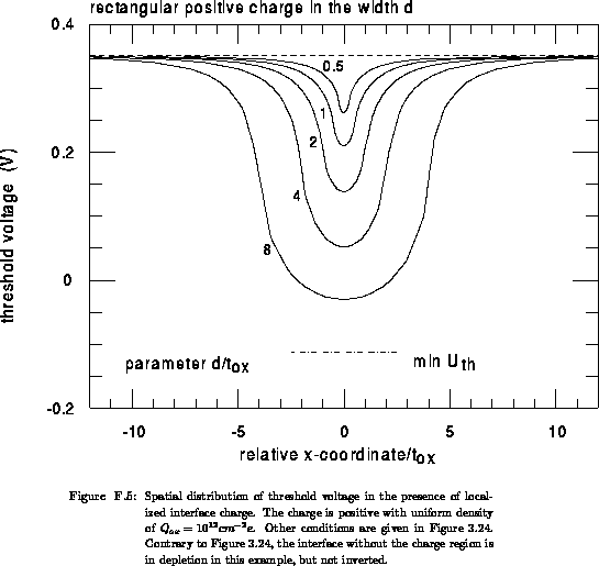
So far we have contemplated on the bulk depletion. In conditions comprised in
the example shown in Figure 3.24 a considerable part of the
interface is inverted. The inversion layer screens the bulk under the localized
charge from possible influences of the gate-bias variations; the screening
reduces the two-dimensional effect under the interface charge. Presently, we
did not develop an appropriate theory to account for the screening
(see [331][40]). Reasoning heuristically, one expects that the
screening attenuates the induced , but increases
with respect to its extreme value. The necessary to induce
 increases in comparison
with the case when the inversion layer vanishes. The bulk capacitance,
consisting of a large inversion-layer capacitance
increases in comparison
with the case when the inversion layer vanishes. The bulk capacitance,
consisting of a large inversion-layer capacitance  and the depletion
capacitance , becomes much larger than . Rigorously considering, the
problem is nonlinear and the moving charge cannot be neglected, as done by
deriving the present theory for . We demonstrate the effect on
two examples. In Figure 3.24 the interface is inverted in
all points whose
and the depletion
capacitance , becomes much larger than . Rigorously considering, the
problem is nonlinear and the moving charge cannot be neglected, as done by
deriving the present theory for . We demonstrate the effect on
two examples. In Figure 3.24 the interface is inverted in
all points whose  is below a specified gate bias, whereas it is
depleted around the central point
is below a specified gate bias, whereas it is
depleted around the central point  , due to negative interface charge.
In Figure F.5 the bulk is inverted in the area surrounding the
point , else it is completely depleted for all points whose is
larger than a specified gate bias, because of positive interface charge. As
arising from numerical modeling, the attenuation of the local threshold-voltage
shift is larger when the interface around the charge is depleted than when it
is inverted, in spite of a larger depletion-layer width assumed in the
calculation in the latter case. As already mentioned, larger leads to
lower . We ascribe this finding to the screening in the former
example.
Although the exact results can be obtained by means of numerical simulation only, because of the screening, the possible lateral current flow and the inhomogeneity in the two-dimensional doping profile, the given analytical models are still a good basis for evolution of the importance of the effect. Further work should cover finding an efficient representation of expression F.21 and simplifying the developed models, in order to make them more appropriate for engineering purposes.