


 CMOS Technology
The motivation given in [139]
for the fully planarized CMOS
technology is twofold. First, the formation of a
shallow junction of less than  depth is problematic with any
thermal cycle, even with Rapid Thermal Processing (RTP)
techniques. This is, however, a requirement for an acceptable short
channel behavior of quarter micron CMOS devices. Using a strongly
recessed poly gate (this implies a nonplanar silicon segment), the
presented technology even achieves junction depths of about
depth is problematic with any
thermal cycle, even with Rapid Thermal Processing (RTP)
techniques. This is, however, a requirement for an acceptable short
channel behavior of quarter micron CMOS devices. Using a strongly
recessed poly gate (this implies a nonplanar silicon segment), the
presented technology even achieves junction depths of about  .
The second feature and motivation of this technology is the
full planarization, enabled by Shallow Trench Isolation
(STI) techniques and by the recessed poly gate.
.
The second feature and motivation of this technology is the
full planarization, enabled by Shallow Trench Isolation
(STI) techniques and by the recessed poly gate.
It will be shown in the simulation that the planarization of the
device surface leads to a highly nonplanar structure in the
(epitactical) silicon segment.
The most characteristic processing steps of the
fully palanarized, shallow-trench-isolated, quarter micron CMOS
technology are depicted in Figures 7.1 to 7.9.
All coordinate values are given in
of the
fully palanarized, shallow-trench-isolated, quarter micron CMOS
technology are depicted in Figures 7.1 to 7.9.
All coordinate values are given in  . The evolution of the
nonplanar silicon segment is emphasized by a bold solid line.
. The evolution of the
nonplanar silicon segment is emphasized by a bold solid line.
The starting material is  epi on heavily doped
  substrate.
A planarized trench isolation is formed by defining a mask
(Figure 7.1), followed by
unidirectional etching of
substrate.
A planarized trench isolation is formed by defining a mask
(Figure 7.1), followed by
unidirectional etching of  deep trenches
into the silicon substrate (Figure 7.2), refilling the trenches
with CVD oxide (Figure 7.3) and planarization (Figure 7.4 and
Figure 7.5). The planarization is accomplished by first spinning
on a resist layer and then etching back using a combination of
Reactive Ion Etching (RIE) and Chemical Mechanical
Polishing (CMP), as described in [140].
deep trenches
into the silicon substrate (Figure 7.2), refilling the trenches
with CVD oxide (Figure 7.3) and planarization (Figure 7.4 and
Figure 7.5). The planarization is accomplished by first spinning
on a resist layer and then etching back using a combination of
Reactive Ion Etching (RIE) and Chemical Mechanical
Polishing (CMP), as described in [140].
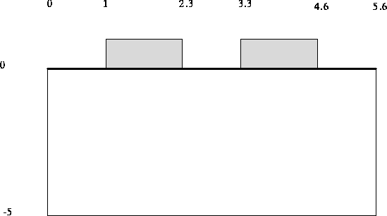
Figure 7.1: Initial device structure with mask for isolation
trench definition
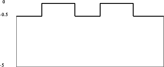
Figure 7.2: Device structure after isolation trench etching
and mask removal
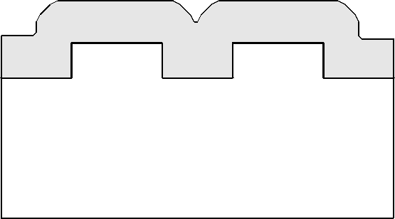
Figure 7.3: Device structure after isotropic oxide deposition
(CVD)
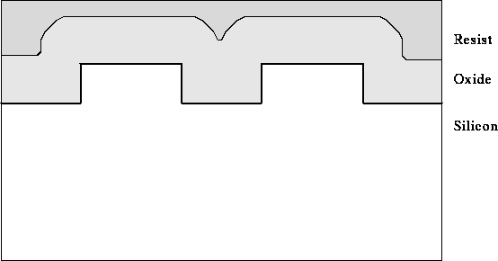
Figure 7.4: Device structure after resist spin-on for planarization
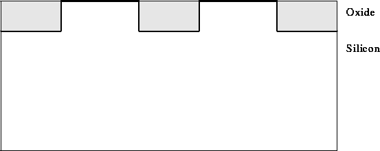
Figure 7.5: Planarized device structure after back-etching of
resist and oxide. Isolation of device regions is provided by three
oxide-filled shallow trenches.
N-well and p-well implants are performed
(Phosphorus and Boron, typically  )
followed by a drive-in cycle (3.5 minutes at
)
followed by a drive-in cycle (3.5 minutes at  C).
C).
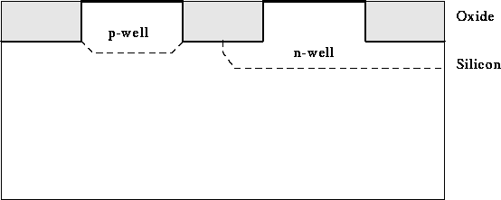
Figure 7.6: Device structure after p-well and n-well implantation
The gate formation starts with a lithographic step to define the gate
opening, then etching a  deep trench into both the silicon
and the oxide isolation areas simultaneously by a
1:1 silicon/oxide etch step.
deep trench into both the silicon
and the oxide isolation areas simultaneously by a
1:1 silicon/oxide etch step.
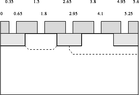
Figure 7.7: Device structure with mask for gate trench etching
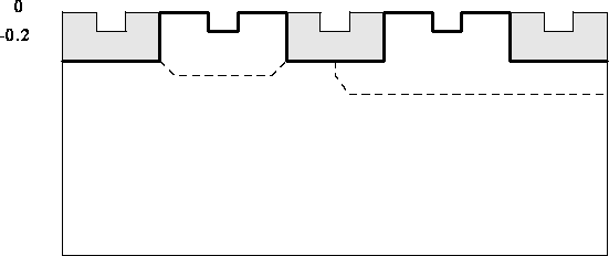
Figure 7.8: Device structure after gate etch step and mask removal
A thin oxide layer is grown thermally and a layer of nitride is deposited and etched back with RIE to form an oxide/nitride sidewall in the silicon trench which reduces gate to junction overlap capacitances. (This detail is not shown in Figure 7.9 and Figure 7.10). The gate oxide is grown, polysilicon is deposited and the structure is planarized as before (Figure 7.9).
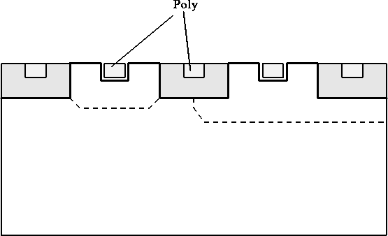
Figure 7.9: Device structure with deposited polysilicon gates
after planarization
To complete the CMOS transistors, the  and junctions are
formed by Arsenic implantation and Germanium preamorphized Boron
implantation, respectively. The poly gates are doped simultaneously
with the junction implantations.
and junctions are
formed by Arsenic implantation and Germanium preamorphized Boron
implantation, respectively. The poly gates are doped simultaneously
with the junction implantations.
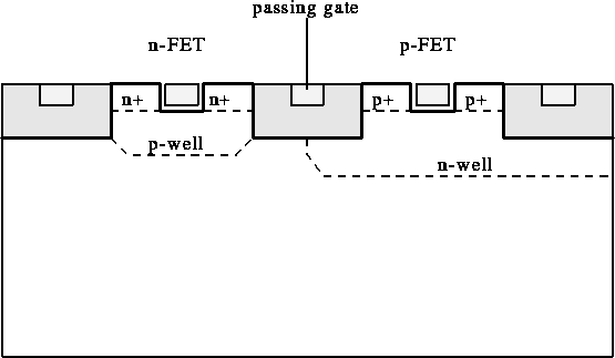
Figure 7.10: Final CMOS structure after junction formation
The device fabrication then continues with passivation, contact hole opening and metallization (not shown). One easily recognizes that in the final structure (Figure 7.10) the poly gate is completely buried in the silicon substrate in both the active device region and the shallow trench isolation region. Because of its perfectly planar surface, the structure is highly suitable for future planarized multi-level metal interconnection approaches.