The presented planarized shallow trench isolated CMOS technology is highly demanding with regard to the integration of topography and doping definition steps. For the simulation of the fabrication process, the challenge lies in the alternating etching/deposition and implantation/diffusion steps. For each step, a specialized process simulation tool must be used and the wafer state must be kept consistent, although each of these specialized tools focuses on a certain aspect and neglects others.
The simulators ETCH [141], TSUPREM-4 [142], the Monte Carlo module of PROMIS for the simulation of ion implantation [94] and the auxiliary tool SKETCH for modeling spin-on, exposure, and mask strip steps are used to simulate the process.
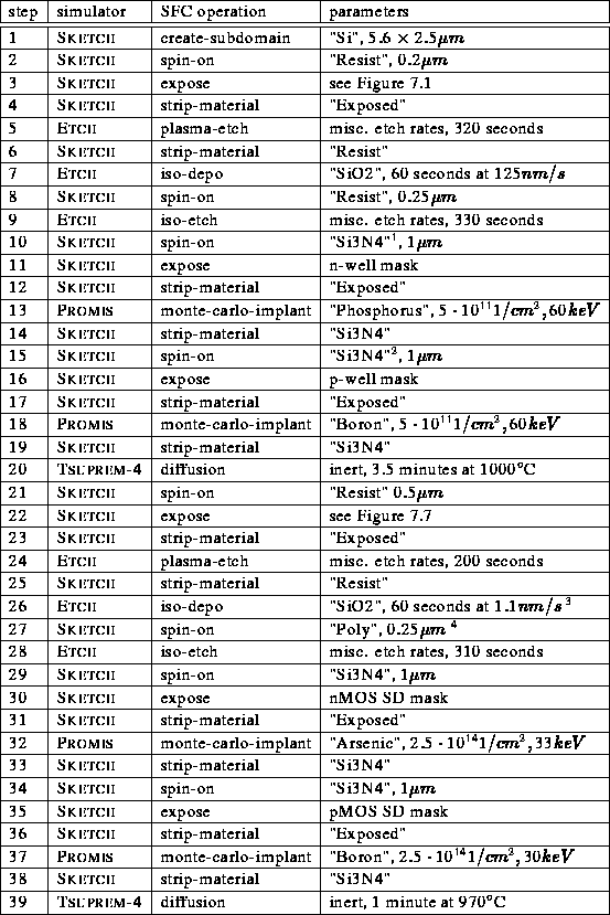
Table 7.1: Process simulation flow for the  , fully planarized,
shallow trench isolated CMOS process.
, fully planarized,
shallow trench isolated CMOS process.
This example process also demonstrates the use of VORONOI within the VISTA framework. The simulation flow employs three entriely different process simulation tools and VORONOI is used repeatedly to achieve consistency between grid and geometry, and to transform the structural and doping information between tool-specific and wafer state compliant form.
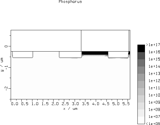
Figure: N-well doping profile (Phosphorus) after ion implantation,
simulated with the PROMIS Monte Carlo ion implantation module.
Result of step 13.
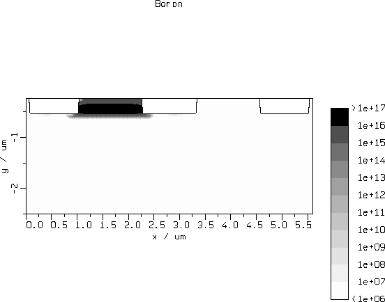
Figure: P-well doping profile (Boron) after ion implantation,
simulated with the PROMIS Monte Carlo ion implantation module.
Result of step 18.
Figure 7.11 and Figure 7.13 show the doping profiles of n-well and p-well after implantation (step 18). VORONOI has already been used to create a geometry-conforming grid and to transfer the doping from the non-geometry-conforming tensor-product grid of the Monte Carlo module for ion implantation onto the triangular grid.
This doping information has been fed into TSUPREM-4 for the simulation of the drive-in diffusion (step 20). The resulting doping profiles of n-well and p-well are shown in Figure 7.13 and Figure 7.14.
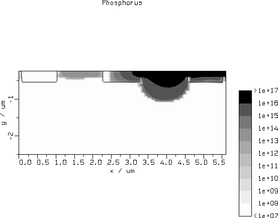
Figure: N-well doping profile after drive-in diffusion,
simulated with TSUPREM-4. Result of step 20
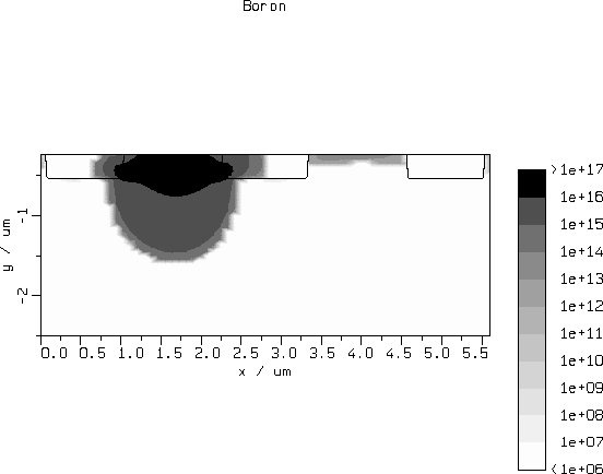
Figure: P-well doping profile after drive-in diffusion,
simulated with TSUPREM-4. Result of step 20
Figure 7.15 shows the Phosphorus doping of the n-well after the trenches for the MOS gates and for the passing gates have been etched. This etch step removes part of the geometry and the grid and doping is ``repaired'' by VORONOI to produce a consistent wafer state.
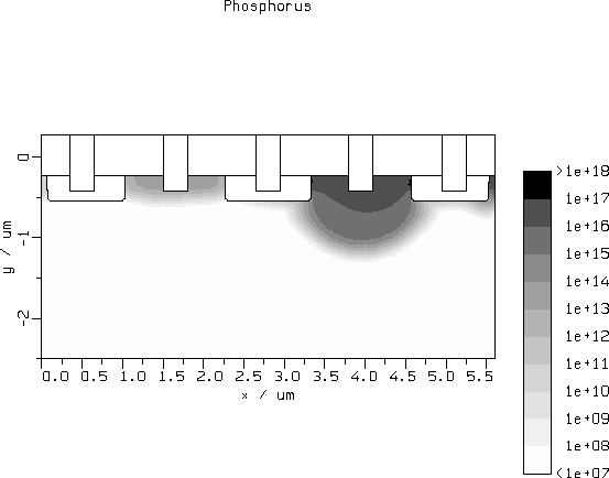
Figure 7.15: N-well doping profile after etching the trench for the planarized
poly gate. Result of step 24
Figure 7.16 is a screen dump of xpif2d showing the final planarized geometrical structure of the nMOS transistor along with the phosphorus concentration before the mask definition for Source / Drain implantation (after step 28).
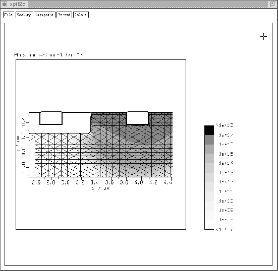
Figure 7.16: xpif2d showing a detail of the n-well and a nearby passing gate
structure. Result of step 28
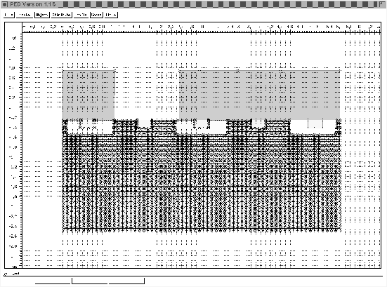
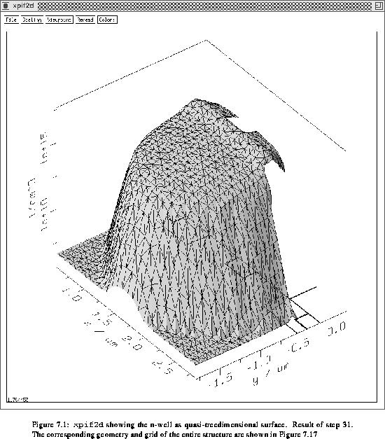
Figure: PED showing the entire CMOS structure with the
grid on the silicon segment,
triangulated by VORONOI.
Result of step 31
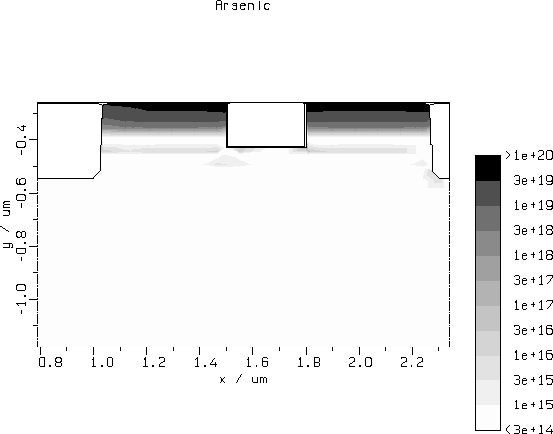
Figure 7.19: Source and drain profiles of the nMOS transistor
after the Monte Carlo simulation of ion implantation. Result of step 38.
Figure 7.19
shows the implanted source and drain doping
profiles of the nMOS transistor. The subsequent final annealing step
(step 39) does not change the form of te profiles. Note that
some local maxima can be observed at a depth of about  , which is
a well-known peculiar effect of the
quantization of ions by the Monte Carlo method.
, which is
a well-known peculiar effect of the
quantization of ions by the Monte Carlo method.