at the same time requires to scale all doping concentrations by
a factor of
at the same time requires to scale all doping concentrations by
a factor of  to maintain the same electric fields inside the device
[2].
to maintain the same electric fields inside the device
[2].
In 1926 Julius Edgar Lilienfeld first described a device similar to what we now call a field effect transistor in the US-patent named “Method and apparatus for controlling electric current” [1]. However, it took about thirty more years until the first transistor was actually built; ironically, it was a bipolar junction transistor.
While the first integrated circuits only contained a few transistors, the
demand for more complex circuits, and therefore a higher number of transistors,
increased steadily. To accomplish the growing number, scaling became the most
important topic. In 1974 Dennard et al. presented a paper where they
stipulated that scaling all device dimensions and voltages by a factor
of at the same time requires to scale all doping concentrations by
a factor of to maintain the same electric fields inside the device
[2].
In the beginning of the 1980s, the complementary metal-oxide-semiconductor (CMOS) technology was introduced to maintain the development of the already “very large-scaled integration” (VLSI) of transistors. Besides decreasing device size, cleaner and larger fabrication plants for semiconductor manufacture (fabs) were required to increase the yield.
As the demand for faster central processing units (CPUs), larger memory
cells, and other integrated circuits increased further, reliability issues concerning
the product specifications became more important. In order to reduce the rate of
failure of devices further, the semiconductor industry had to improve the involved
production processes which often included the replacement of materials
responsible for the malfunction of devices. Unfortunately the novel materials in
turn caused reliability challenges. One of these reliability phenomena was
originally discovered in 1966, when Miura et al. linked the generation of
charge due to an electrochemical reaction to the presence of a strong
electric field at the Si– interface [3], a phenomenon called bias
temperature instability (BTI). Despite this, BTI was nearly forgotten for
some decades due to its only minor relevance for the early semiconductor
industry.
interface [3], a phenomenon called bias
temperature instability (BTI). Despite this, BTI was nearly forgotten for
some decades due to its only minor relevance for the early semiconductor
industry.
Already right from the start, it was discovered that when interfacing different
materials with different lattice parameters, like Si and  , defects maybe
generated at the interface [3, 4]. This is due to the non-abrupt transition,
which spans over one to two atomic layers and results in an “interface
region”, where a lot of dangling bonds act as traps for electrons and
holes. By annealing of the structure with hydrogen (H-passivation) the
density of these dangling bonds at the interface
, defects maybe
generated at the interface [3, 4]. This is due to the non-abrupt transition,
which spans over one to two atomic layers and results in an “interface
region”, where a lot of dangling bonds act as traps for electrons and
holes. By annealing of the structure with hydrogen (H-passivation) the
density of these dangling bonds at the interface  can be reduced
from
can be reduced
from  to around
  [5], which is a huge
improvement. When placing a metal gate electrode on top of the
[5], which is a huge
improvement. When placing a metal gate electrode on top of the  -oxide, a
metal-oxide-semiconductor (MOS) structure is formed, whose operation is
explained in Appendix B. Such a MOS-structure is the central part in the
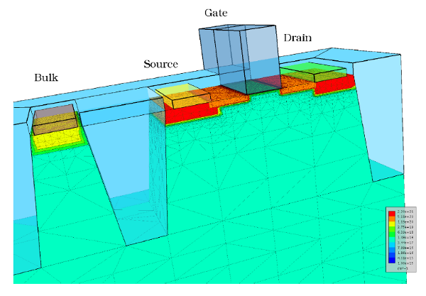
metal-oxide-semiconductor field effect transistor (MOSFET), which is
exemplarily shown in Fig. 1.1.
-oxide, a
metal-oxide-semiconductor (MOS) structure is formed, whose operation is
explained in Appendix B. Such a MOS-structure is the central part in the
metal-oxide-semiconductor field effect transistor (MOSFET), which is
exemplarily shown in Fig. 1.1.
As already mentioned, newer materials entered the MOSFET-structure and especially the gate oxide. With the introduction of nitrogen into the oxide the permittivity was increased and the boron diffusion from the gate material into the bulk semiconductor was significantly reduced. At the same time BTI increased in importance1 .