 , is zero [10].
The operating conditions depend on the applied voltage
, is zero [10].
The operating conditions depend on the applied voltage  on the metal
contact with respect to the Fermi level of the grounded semiconductor and
are called accumulation (a), flatband (b), depletion (c), and inversion
(d).
on the metal
contact with respect to the Fermi level of the grounded semiconductor and
are called accumulation (a), flatband (b), depletion (c), and inversion
(d).
The band diagrams of an ideal MOS structure consisting of a gate electrode
(metal or polysilicon), a dielectric (oxide), and a semiconductor (nMOS or
pMOS) are shown in Fig. B.1 under different operating conditions for both
nMOS and pMOS. For the most simple case it is assumed that (i) there are no
charges in the oxide, (ii) the resistivity of the oxide is infinite, and (iii) the work
function difference between the metal and the semiconductor, , is zero [10].
The operating conditions depend on the applied voltage on the metal
contact with respect to the Fermi level of the grounded semiconductor and
are called accumulation (a), flatband (b), depletion (c), and inversion
(d).
In the following the pMOSFET with n-substrate will be explained:
(a) When a positive voltage is applied at the contact the conduction band
 bends down towards the Fermi level
  that is set constant in the
semiconductor where no current flows. This bending yields an accumulation of
the majority carriers (electrons) near the interface.
that is set constant in the
semiconductor where no current flows. This bending yields an accumulation of
the majority carriers (electrons) near the interface.
(b) For  all bands remain flat and the semiconductor and its majority
and minority carriers are in thermal equilibrium.
all bands remain flat and the semiconductor and its majority
and minority carriers are in thermal equilibrium.
(c) Under a small negative voltage the majority carriers are repelled from the
interface, involving that the bands are bend up. The intrinsic energy  gets
closer to
gets
closer to  .
.
(d) When further increasing the negative voltage this bending continues and
once  crosses
  the minority carriers (holes) exceed the majority carriers
at the interface. Hence, this case is called inversion, as the interface is
inverted.
the minority carriers (holes) exceed the majority carriers
at the interface. Hence, this case is called inversion, as the interface is
inverted.
For the p-type structure with holes as majority carriers and electrons as minority carriers only the polarity of the voltage has to be changed.
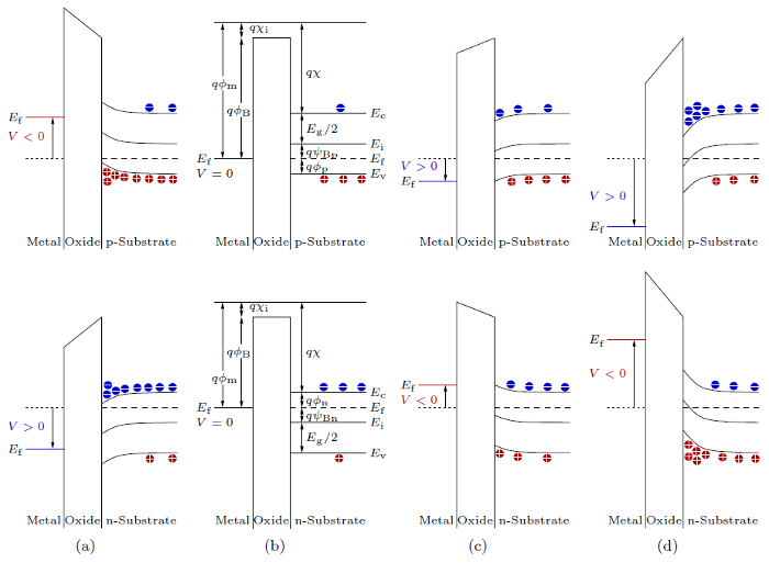
 and
downwards if
and
downwards if  . The energy levels and potentials are marked for
the flatband condition (
. The energy levels and potentials are marked for
the flatband condition ( ), with
  denoting the Fermi potential
with respect to the vacuum level,
denoting the Fermi potential
with respect to the vacuum level,  and
and  , as electron affinity for the
oxide and the substrate, and
, as electron affinity for the
oxide and the substrate, and  as bandgap in the substrate. Top: For a
p-semiconductor (nMOS) it holds that
as bandgap in the substrate. Top: For a
p-semiconductor (nMOS) it holds that  ,
where
,
where  and
and  represent the Fermi potentials with respect to
the intrinsic energy
represent the Fermi potentials with respect to
the intrinsic energy  and valence band
  . Bottom: For an
n-semiconductor (pMOS) one obtains
. Bottom: For an
n-semiconductor (pMOS) one obtains  with
with  and
and  as the Fermi potentials with respect to the conduction band
  and intrinsic energy
  .
.