 and stress voltages
  is essential. This measurement data is
then fitted by using a single parameter set. Eventually, the calibrated parameter
set is shown in the following to successfully account for all performed
measurements.
is essential. This measurement data is
then fitted by using a single parameter set. Eventually, the calibrated parameter
set is shown in the following to successfully account for all performed
measurements.
To validate the multi-state defect model described in the last section,
experimental data with logarithmically increasing stress times for different
temperatures and stress voltages is essential. This measurement data is
then fitted by using a single parameter set. Eventually, the calibrated parameter
set is shown in the following to successfully account for all performed
measurements.
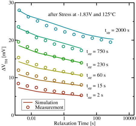
For a given temperature and voltage, as illustrated in Fig. 9.9, it is possible
to simulate a complex eMSM-sequence, consisting of logarithmically increasing
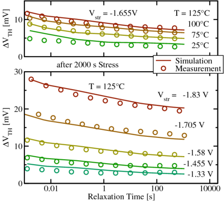
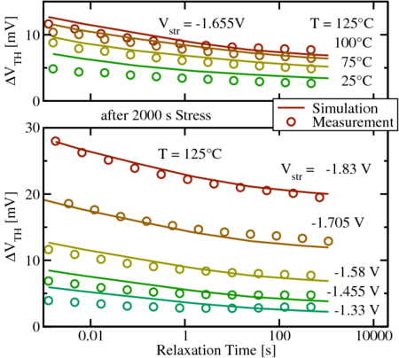
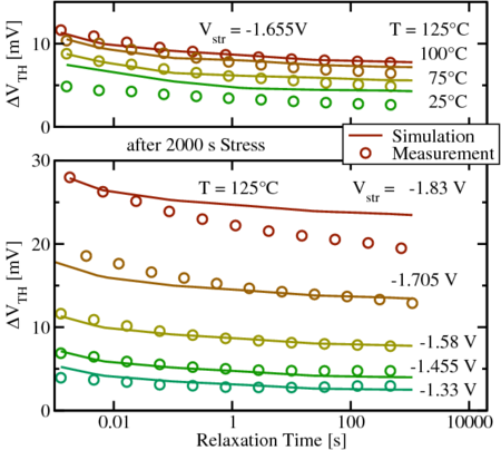
stress times, with very good agreement. Furthermore, the last relaxation
sequence after more than  of stress is compared at different temperatures
and for different stress voltages, cf. Fig. 9.10. Despite device to device deviations,
as various MOSFETs have to be used for the measurements to avoid pre-stress,
it can be clearly seen that the measurements are very well reproduced
using the multi-state defect model in combination with a broad defect
distribution.
of stress is compared at different temperatures
and for different stress voltages, cf. Fig. 9.10. Despite device to device deviations,
as various MOSFETs have to be used for the measurements to avoid pre-stress,
it can be clearly seen that the measurements are very well reproduced
using the multi-state defect model in combination with a broad defect
distribution.
It was already mentioned that an investigation of the time dependence of a
single defect is not reasonable in large device. However, the relaxation behavior
observed in Fig. 9.9 and Fig. 9.10 can be modeled by the superposition of
defects with different emission time constants. This is confirmed by Fig. 9.6,
where the percentage of the charged oxide defects is correlated with the last
relaxation sequence for  and
and  . At the beginning of the
relaxation
. At the beginning of the
relaxation  of the possible defects contribute, while after about
  relaxation only
  are left, which is equivalent to nearly complete relaxation of
the switching traps. The permanent part left can be explained by recalling
the two-stage model [98], which assumes depassivated interface states
contributing to the permanent part of NBTI (Fig. 9.10). In the simulation the
permanent part was modeled by an additional defect level which can
only be filled during stress. During recovery the defect level remains
occupied.
are left, which is equivalent to nearly complete relaxation of
the switching traps. The permanent part left can be explained by recalling
the two-stage model [98], which assumes depassivated interface states
contributing to the permanent part of NBTI (Fig. 9.10). In the simulation the
permanent part was modeled by an additional defect level which can
only be filled during stress. During recovery the defect level remains
occupied.
A further issue when dealing with device simulations was the already mentioned exactness of the distributions due to the different amount of taken defects. Here a number of 1000 representative defects exhibits a good compromise between computational efforts and accuracy of the simulation when fitting the experiments. Therefore this value is chosen for the calibration of the parameter set. When taking more defects into account, the simulation results become smoother and do not contain the small kinks, as visible in Fig. 9.10 for 1000 defects. However, this is only due to numerical reasons, since the actual degradation is always obtained by scaling the behavior of the “respresentative” defects. Consequently, the overall behavior is not changed, which can be seen when comparing Fig. 9.10 and Fig. 9.11.
At last, it can be pointed out that the classical approach, which assumes all
holes to be energetically located at the valence band edge of the substrate, shows
small deviations from the QM-results, especially for  and
and  ,
cf. Fig. 9.12. This is due to the missing influence of the subbands which are
localized in the SiGe-layer.
,
cf. Fig. 9.12. This is due to the missing influence of the subbands which are
localized in the SiGe-layer.
 and
and
 ) the classical approach can as well be applied and
yields rather good agreement with the experiment.
) the classical approach can as well be applied and
yields rather good agreement with the experiment.