Chapter 9
Modeling NBTI in High-k SiGe pMOSFETs
In the last chapter it was concluded that the recovery after BTI is the mere
consequence of single defects being discharged at certain emission times, which
gives a step-like drain current behavior in small devices. The superposition of
many of these defects, as observed in large-area devices, yields the typical log-like
recovery behavior[11]. The latest attempt to model such defects is based on the
non-radiative multi-phonon emission (NMP) theory after [153, 125, 124], cf.
Chapter 8.5.3. This theory assumes the conservation of the total energy of a
defect or defect system consisting of a strongly coupled electronic and vibronic
part [130].
In [111] the NMP model was already shown to successfully reproduce
measurement data of small-area devices containing only a few defects. In this
chapter it will be shown that the theory also holds for rather complex large-area
p-MOSFETs containing a larger number of defects. Such devices have been
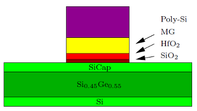
studied by Franco et al. [164, 165] and feature a buried SiGe channel with a
thick SiGe quantum well of high Ge-fraction ( ) and a thin silicon
cap below the high-k dielectric in order to reduce NBTI. This type of
device is schematically depicted in Fig. 9.1. Devices of this kind were
subjected to NBTI stress using various stress voltages and temperatures
via the extended measure-stress-measure routine after [18]. For this, a
static
) and a thin silicon
cap below the high-k dielectric in order to reduce NBTI. This type of
device is schematically depicted in Fig. 9.1. Devices of this kind were
subjected to NBTI stress using various stress voltages and temperatures
via the extended measure-stress-measure routine after [18]. For this, a
static  -characteristic is taken first to obtain a reference. After the
stress sequences with logarithmically increasing stress times from
-characteristic is taken first to obtain a reference. After the
stress sequences with logarithmically increasing stress times from  to
to  the degraded threshold voltage is monitored with a delay of
 .
.