6.3.2 Temperature Scaling
The temperature dependence of  is displayed in Fig. 6.11 (top)
for the thinnest device (
is displayed in Fig. 6.11 (top)
for the thinnest device ( ) with
 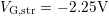 . In the
range
. In the
range  to
to  , the data can be perfectly fit by a logarithmic
time dependence (differences would not even be visible in the plots). A
slight deviation is observed for higher temperatures for
, the data can be perfectly fit by a logarithmic
time dependence (differences would not even be visible in the plots). A
slight deviation is observed for higher temperatures for  ,
possibly due to the onset of the mechanism responsible for the long-time
power-law behavior with a larger power-law exponent
,
possibly due to the onset of the mechanism responsible for the long-time
power-law behavior with a larger power-law exponent  . This
might be due to the dependence of two compound power-laws which are
discussed in literature [49]. Apart from that, different temperatures can
be scaled well to the data at
. This
might be due to the dependence of two compound power-laws which are
discussed in literature [49]. Apart from that, different temperatures can
be scaled well to the data at  , as shown by the dotted
lines in Fig. 6.11 (top), and the indicated scaling factors marked by
arrows.
, as shown by the dotted
lines in Fig. 6.11 (top), and the indicated scaling factors marked by
arrows.
 ,
,  ,
,  , and
, and  ) and
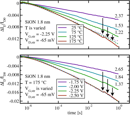
voltage dependence (
) and
voltage dependence ( ,
,  ,
,  , and
, and  ) of
) of
 degradation. Scaling to the dotted lines works perfectly for
various stress voltages at equal temperatures, while different temperatures
lead to a small deviation for
degradation. Scaling to the dotted lines works perfectly for
various stress voltages at equal temperatures, while different temperatures
lead to a small deviation for  . The scaling factors are also given.