Since the ![]() -distribution is only a virtual model parameter, the width of the reaction layer does not agree with the thickness of the real physical interface between silicon and SiO
-distribution is only a virtual model parameter, the width of the reaction layer does not agree with the thickness of the real physical interface between silicon and SiO![]() . In the calculated
. In the calculated ![]() -distribution the reaction layer normally ranges over some finite elements (see Fig. 6.4), but in reality the Si/SiO
-distribution the reaction layer normally ranges over some finite elements (see Fig. 6.4), but in reality the Si/SiO![]() -interface is only a few atom layers thick.
So for a more physical presentation of the (final) simulation result a sharp interface between silicon and SiO
-interface is only a few atom layers thick.
So for a more physical presentation of the (final) simulation result a sharp interface between silicon and SiO![]() must be constructed.
must be constructed.
For the sake of simplicity the splitting procedure is demonstrated on a two-dimensional grid example. The simulated structures are three-dimensional with a tetrahedral mesh, but the principle is the same as with triangles. The left side of Fig. 6.5 shows a subarea of a mesh with the ![]() -values on the nodes. There the
-values on the nodes. There the ![]() -values on the upper nodes are less than 0.5 and on the lower nodes are higher than 0.5. This means that the virtual surface with
-values on the upper nodes are less than 0.5 and on the lower nodes are higher than 0.5. This means that the virtual surface with ![]() must be located somewhere between the upper and lower nodes. The position of
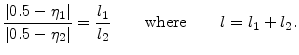
must be located somewhere between the upper and lower nodes. The position of ![]() on each element edge can be calculated with the known values
on each element edge can be calculated with the known values ![]() and
and ![]() on the two corresponding nodes
on the two corresponding nodes
After the position of ![]() is calculated on an edge, a new node is inserted and the edge is split into two parts. The new nodes are marked with red color in the right side of Fig. 6.5. With the help of additional nodes, which are not placed on the egdes, a local remeshing of the interface grid can be performed, which results in two separated segments for silicon and SiO
is calculated on an edge, a new node is inserted and the edge is split into two parts. The new nodes are marked with red color in the right side of Fig. 6.5. With the help of additional nodes, which are not placed on the egdes, a local remeshing of the interface grid can be performed, which results in two separated segments for silicon and SiO![]() with a sharp interface. The mesh operations for this segment splitting were implemented in FEDOS.
with a sharp interface. The mesh operations for this segment splitting were implemented in FEDOS.
Another problem associated with segment splitting is that the generated interface is not smooth, especially in critical regions or where it has a curvature. The reasons are numerical inaccuracies which come from the finite element discretization, but also from the Newton solving method because both are approximation methods. After a number of simulation loops (see Section 6.2) the inaccuracies sum up and lead to visible differences in the ![]() -distribution.
-distribution.
The situation after the segment splitting of the oxidized structure from Fig. 6.4 is shown in Fig. 6.6. Only the silicon segment (with the same proportions) is presented. Although the mesh has good quality, the interface is craggy because of the previously described problems. For a more realistic Si/SiO![]() -interface the quality of its curvature and mesh can be improved with an additional smoothing routine.
-interface the quality of its curvature and mesh can be improved with an additional smoothing routine.
The smoothing algorithm is implemented in the WAFER-STATE-SERVER in form of advanced GTS-functions [106]. The basic idea of the smoothing model is to move all points which are connected to artificial edges. An important part is to select which surface points belong to natural edges of the structure and which to artificial ones [107]. The principle of the point selection method can be explained with the help of Fig. 6.7. Points on planar surfaces like P![]() can be excluded from the smoothing process, because they are only surrounded by planar triangles. The same is valid for points like P
can be excluded from the smoothing process, because they are only surrounded by planar triangles. The same is valid for points like P![]() , which are located on natural edges, because they are also connected with at least one planar surface.
, which are located on natural edges, because they are also connected with at least one planar surface.
The best strategy for finding a point as P![]() , which needs smoothing, is to check the surface curvature. A typical property of a point on an artificial edge is that the curvature of at least one connected other point is opposite. Such switching curvature can be located straightforwardly, with an angle criterion. As demonstrated in Fig. 6.7 the angle between the triangles at point P
, which needs smoothing, is to check the surface curvature. A typical property of a point on an artificial edge is that the curvature of at least one connected other point is opposite. Such switching curvature can be located straightforwardly, with an angle criterion. As demonstrated in Fig. 6.7 the angle between the triangles at point P![]() is acute (
is acute (
![]() ), but the angle at the connected point is obtuse (
), but the angle at the connected point is obtuse (
![]() ). A plausible criterion for switching curvatures is to analyze, if the angles of connected points switch between less 180
). A plausible criterion for switching curvatures is to analyze, if the angles of connected points switch between less 180![]() and greater 180
and greater 180![]() . It can be found with this criterion that point P
. It can be found with this criterion that point P![]() belongs to an already smooth surface, because both angles
belongs to an already smooth surface, because both angles ![]() and
and ![]() have similar values less than 180
have similar values less than 180![]() (
(
![]() ).
).
After selection of the points which have to move, their distances and directions of motion are another important aspects [107]. At first, the maximally allowed sphere of the motion of a point around its original position is given by the shortest distance to its connected points, as displayed in Fig. 6.8. Since the smoothing process is performed with a number of iterations, the distance of motion within each iteration loop is set to
![]() or less of the respective sphere radius. The direction of motion for a point for each iteration loop is calculated as the sum of normals of all triangles connected to this point (see right hand side in Fig. 6.8). The smoothing process for the selected points is stopped, if the difference of the angles between connected points is within a (small) tolerance.
or less of the respective sphere radius. The direction of motion for a point for each iteration loop is calculated as the sum of normals of all triangles connected to this point (see right hand side in Fig. 6.8). The smoothing process for the selected points is stopped, if the difference of the angles between connected points is within a (small) tolerance.
The simulation results of the oxidation process after the previously described segment splitting and smoothing procedure (see Fig. 6.4), are presented with a more physical sharp interface between the SiO![]() - and silicon segment in Fig. 6.10. It is worth mentioning that all pictures of this oxidation example have same proportions and perspectives for optimal comparison.
- and silicon segment in Fig. 6.10. It is worth mentioning that all pictures of this oxidation example have same proportions and perspectives for optimal comparison.
![\includegraphics[width=0.95\linewidth]{fig/cutgrid}](img807.png)
![\includegraphics[width=0.7\linewidth]{/iuehome/hollauer/work3/oxidwCutaP/1000Cb/old/beforesmooth-lightwxv.ps}](img808.png)
![\includegraphics[width=0.8\linewidth]{fig/smooth1}](img809.png)
![\includegraphics[width=0.85\linewidth]{fig/smooth2a}](img817.png)
![\includegraphics[width=0.7\linewidth]{/iuehome/hollauer/work3/oxidwCutaP/1000Cb/old/aftersmooth-lightwxv.ps}](img818.png)
![\includegraphics[width=0.7\linewidth]{/iuehome/hollauer/work3/oxidwCutaP/1000Cb/old/sharp-lightwxv.ps}](img819.png)