Chapter 5
Impact of Charged Traps and Random Dopants on the Performance of Si MOSFETs
Charged traps near the oxide/silicon interface and in the oxide bulk can have a dramatic impact on the characteristics of
MOSFETs [107, 37, 109, 10, 105, 65, 159, 90, 63, 168, 166]. Although nanoscale transistors contain very few
defects [90], each can significantly disturb the channel electrostatics and affect device performance. Particularly, the lifetime
of a device [166, 37] is ultimately determined by the time-dependent variability of the transistor characteristics. Such
time-dependent variability is caused by the creation/annealing and/or the charging/discharging of interface
and oxide traps. Consequently, one must study device reliability from a statistical point of view. Therefore,
recently much information on the energy levels of border traps [45, 168, 166] and their depth distribution
in the oxide film [105] has been presented. However, the information on the lateral defect position is also
important since this would allow for understanding of the role of each single trap in its contribution to the device
performance. That is because charged traps situated in different regions of the device may have a significantly
different impact on the channel electrostatics, depending on the applied bias conditions and the distribution of
random dopants along the channel. Nevertheless, there is no study which would fully describe the impact of the
lateral defect position in the presence of random dopants. Thus in the course of this chapter we will perform a
detailed analysis of this issue and introduce a new method allowing for a precise evaluation of the lateral trap
coordinate.
5.1 Previous Descriptions and their Disadvantages
The impact of the lateral position of a single defect on the device performance was first reported in [10]. The authors of [10]
showed that the amplitude of random telegraph noise (RTN) associated with the charging/discharging of a single trap is
strongly correlated with the lateral coordinate and reaches its maximum when the trap is situated in the middle of the
channel. While the impact of random dopants has been accounted for in their 3D atomistic simulations, the main goal
of [10] was to demonstrate that single defects have a dramatic impact on the performance of ultra-scaled devices. At the
same time, in [10] no significant attention was paid to the experimental evaluation of the lateral defect coordinate.
Nevertheless, the idea to determine the lateral trap position from the analysis of the RTN signal was further developed in
the works [105, 93, 25, 137, 78, 94]. The authors of [105] attempt to extract lateral and depth positions
of the traps from the analysis of gate and drain current RTN. However, the equation which is used for the
estimation of the lateral trap position does not account for the impact of border traps and random dopants
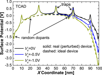
on the shape of the potential profile. In Figure 5.1 we demonstrate that this effect may significantly affect
the shape of the channel barrier, making the results questionable. A similar methodology disregarding the
impact of random dopants is used in [93, 25, 137, 94], while the authors of [78] introduce a 2D trap profiling
technique based on the drain-induced barrier lowering (DIBL) effect [78]. This method employs a relation
between the position of the channel barrier peak and the magnitude of RTN. However, the perturbations of the
surface potential induced by traps and random dopants (Figure 5.1) are also disregarded. This would make the
relation for the peak position evaluated in [78] inapplicable, independently of the magnitude of the DIBL
effect.
In the following we will present a new approach which exploits the fact that the impact of the lateral defect coordinate
XT on the drain bias dependence of the threshold voltage shift ΔV th induced by a single charged trap is stronger than the
impact of random dopants. Accounting for the effect of random dopants is the key feature of our method since it allows us to
estimate the evaluation uncertainty for each of the extracted lateral trap positions. Next we will introduce a compact model
allowing us to understand the underlying physical nature. Finally, we will present a simple equation, which with reasonable
accuracy allows for the estimation of the lateral trap position directly from the experimental data given in
Figure 5.2.
5.2 Experimental Technique
p-MOSFETs with a channel length of L=100nm, a width of W=150nm and a 2.2nm thick SiON gate insulator have been
characterized using TDDS [68, 67, 181]. This technique is based on alternatively charging and discharging preexisting
border traps in order to study their capture and emission times. While having the same properties as newly created
defects [70], in p-MOSFETs these traps are responsible for the recoverable component of the NBTI. By analyzing the TDDS
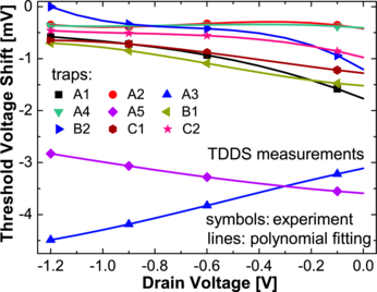
results, the threshold voltage shift ΔV th induced by each particular trap can be individually traced versus the applied drain
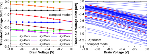
bias V d. Results for three different devices and nine defects are summarized in Figure 5.2. One can see that
the ΔV th(V d) characteristics of every single trap have dramatically different shapes. Since the trap depth
and energy level have no significant impact on the drain bias dependence of ΔV th [57], this indicates that
the traps responsible for the threshold voltage shift are located in different regions of the device [10]. Based
on this assumption, we perform a parameterization of the ΔV th(V d) curves and demonstrate that they can
be perfectly approximated by a cubic polynomial function ΔV th(V d)=∑
ipiV di. As will be shown later, the
corresponding parameterization coefficients are unique for each particular trap position. Therefore, this unique set
of coefficients can be treated as the defect signature and used for a precise evaluation of the lateral defect
coordinate.
5.3 TCAD Simulations
We apply our TCAD simulator Minimos-NT, which considers random discrete dopants using the established methodology
pioneered by Asenov [9] with a density gradient model [5] to account for the quantum correction of the Coulomb
potential [19]. This simulator has already been successfully applied to assess the reliability of modern nanoscale
devices [15, 16]. TCAD simulations were carried out for one hundred p-MOSFETs with identical architectures but with
different configurations of random dopants. Initially we performed the simulations for a fixed coordinate along the
oxide/silicon interface (XT) and different trap positions in the direction perpendicular to the source-bulk-drain plane (WT).
The ΔV th values induced by the traps situated in each particular position were evaluated as a function of V d for all 100
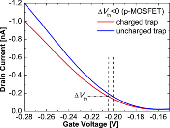
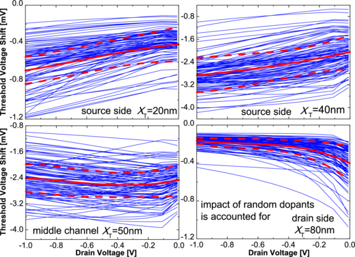
devices using Id-V g curves simulated with and without charged traps. As shown in Figure 5.3, ΔV th was determined
using a standard method [89] for a fixed drain current Id corresponding to V g≤V th, i.e. weak inversion. In
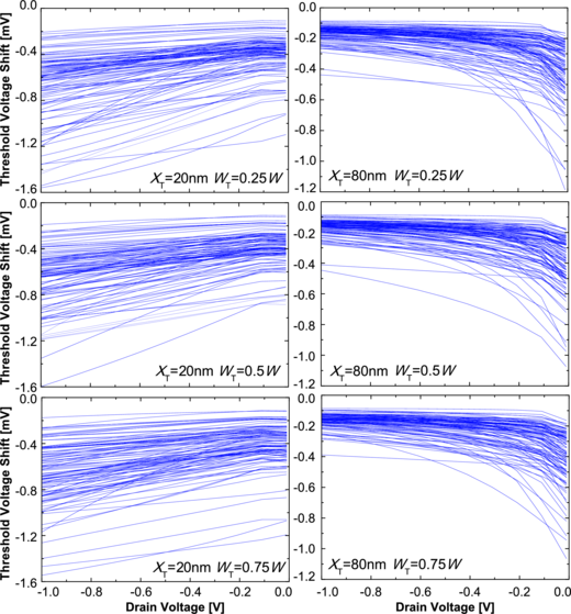
Figure 5.4 it is shown that the position across the channel WT has no significant impact on the shape of the
ΔV th(V d) curves, which implies that WT can not be extracted using our methodology. At the same time, a weak
dependence of the results on WT together with an insignificant impact of the vertical trap position on the
ΔV th(V d) dependence [57] means that the impact of shallow trench isolation [106] on our results is also
negligible. Therefore, in all the following simulations we used WT=W∕2. The lateral defect coordinate XT
was varied from the source to the drain using 10nm steps to provide the benchmark for our trap location
technique.
The obtained ΔV th(V d) curves show a cubic behavior, just like their experimental counterparts. In Figure 5.5 one can
clearly see that the shape of these curves has a stronger dependence on the lateral defect coordinate XT than on the
distribution of random dopants. For example, if a trap is situated at the source side of the channel (XT=20nm and
XT=40nm), ΔV th versus V d increases independently of the configuration of random dopants. However, for a trap situated at
the drain side (XT=80nm) ΔV th versus V d decreases. When a trap is located in the middle of the channel (XT=50nm), the
situation becomes more complicated. Although for most of the random dopant configurations the dependence of ΔV th on V d
is mostly dominated by the higher order polynomial terms, for some of them ΔV th increases versus V d while for others it
decreases. This is because the transition between the two possible types of ΔV th(V d) dependence takes place for trap
positions close to the middle of the channel, although the exact point is determined by the random dopant
configuration.
The observed correlation between the ΔV th(V d) characteristics and the lateral trap position is the key result of our
TCAD simulations. This outcome is in agreement with the experimental results (Figure 5.2). Therefore, this feature
introduces the working principle of our trap location technique. At the same time, the obtained results allow us to conclude
that the expected accuracy of our technique for the central traps is lower because the dependence of the ΔV th(V d) behavior
on the random dopant configuration is strongest.
5.4 Compact Model
The use of TCAD allows for the simulation of the reference data for the trap location technique with rather
high accuracy. However, a physical explanation of the results is not obvious. Therefore, we attempted to
reproduce the observed behaviour of the ΔV th(V d) curves for different XT using a physics based compact
model.
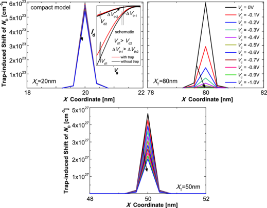
Figure 5.9: In our compact model the impact of a charged border trap is treated as an artificial δ-like local
increase of the channel doping level ND. Its magnitude can be calculated for any XT using the surface potential
distribution along the channel. When the trap is situated at the source side of the channel the concentration shift has
a weak dependence on V d. Therefore, the behaviour of the ΔV th(V d) curves is mainly determined by Id-V g vs. V d
dependence (inset) which leads to a positive slope. Conversely, a strong decrease of the concentration shift induced
by the traps situated at the drain side versus V d leads to ΔV th(V d) curves going down. At the same time, the
charged trap in the middle of the channel is equivalent to a larger concentration shift which leads to a bigger ΔV th.
These dependences are introduced into the simulations based on the Enz-Krummenacher-Vittoz (EKV) model [8]
to obtain the Id-V g characteristics.
Our compact model exploits the fact that the impact of a charged trap on the device electrostatics is equivalent to a local
perturbation of the majority carrier concentration (electrons in the case of p-MOSFETs). This feature is
included by perturbing the surface potential and treating it as a local abrupt increase of the channel doping
level ΔND. The shift of an electron concentration induced by a charge at zero drain bias can be written
as
 | (5.1) |
where ψs0(x)=ψ
s(x, V d=0) is the surface potential along the interface in the absence of a charged defect and
ψsT0(x)=ψ
sT (x, V
d=0) is a peak function centered at x=XT which describes the local shift of ψs0(x) in the presence of a
charged trap (these are the spikes illustrated in Figure 5.1).
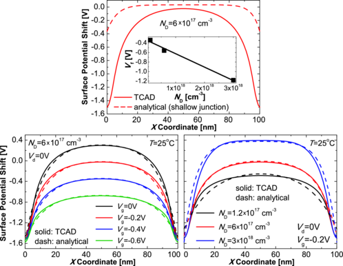
The surface potential distribution ψs0(x) in the absence of the charged trap is calculated using an analytical
model [188]. This model assumes that both source and drain junction depths are negligibly small, which allows us
to avoid a numerical solution of the Poisson equation and derive an analytical expression for the surface
potential. However, ψs0(x) obtained using the original expression from [188], is significantly flattened compared
to its counterpart simulated with TCAD (Figure 5.6). Therefore, we adjusted the model [188] for the case
of a deep junction by neutralizing the shallow junction depth approximation. This was done by artificially
substituting the flat band voltage as V fb=V f-V g and multiplying the built in potential V bi by factor b=3.1,
which is equivalent to an increase in the junction depth yd. As shown in Figure 5.6, this allowed us to obtain
reasonable fits of the surface potential distribution to our TCAD results for different ND and V g. Also, the
fitting parameter b was found to be independent of ND, V g and V d, while V f linearly decays for larger ND
(inset).
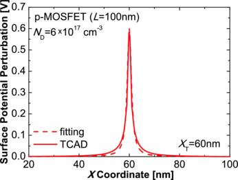
The trap-induced perturbation ψsT0(x) was found to have a universal shape for each device. As shown in Figure 5.7, it
can be accurately fit using a Voigt-like peak function:
 | (5.2) |
Here a plus sign must be taken for a p-MOSFET and a minus sign for an n-MOSFET; the normalization factor is
x0=1nm. The calibration parameter V 0 which determines the spike height is independent of XT and V d
and has to be adjusted to match the obtained ΔV th with their experimental or TCAD counterparts. By
performing the TCAD simulations for different ND we found that typical values of V 0 lie within the range of
0.4–1V.
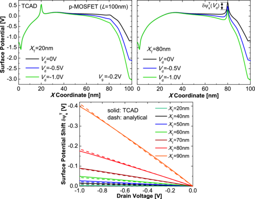
The description above corresponds to the case of zero drain voltage, while simulations of the ΔV th(V d) curves require
incorporation of a V d dependence into the compact model. In the case of an unperturbed surface potential ψs(x, V d) can be
reasonably described using the model [188] which has been used to calculate ψs0(x). However, the channel doping shift ΔN
D
is an exponential function of the surface potential. Therefore, its V d dependence is mainly determined by the behaviour of
the total shift of the surface potential ψsT (x, V
d)=ψsT0(x)+δψ
sT(X
T, V d), where δψsT(X
T, V d) is the V d-induced surface
potential perturbation. The behaviour of δψsT(X
T, V d) can be captured analytically using the approach proposed in [86],
which considers the surface potential distribution in the MOSFET channel with perturbed region. In order to
do this, we adjusted the model [86] to the case of a single defect by assuming that the dimension of the
perturbed area is equal to the lateral size of the trap (see the details in [11]). As shown in Figure 5.8, this
allowed us to reasonably reproduce both XT and V d dependences of δψsT simulated with TCAD. Namely, the
dependence of δψsT on V
d is linear and becomes more pronounced if the trap is situated at the drain side of the
channel.
As was shown above, the quantities ψs0(x), ψ
sT0(x) and δψ
sT(X
T, V d) can be calculated analytically. Therefore, the equivalent
doping level shift is
 | (5.3) |
The doping level profiles obtained for three different trap positions are shown in Figure 5.9, where one can see that ΔND
heights and V d dependences are strongly linked to the lateral trap position. For example, the impact of traps situated in the
middle of the channel (XT=50nm) is equivalent to a much higher doping level shift than it would be for
traps situated closer to the electrodes. At the same time, the concentration shifts, which correspond to traps
situated symmetrically with respect to the middle of the channel (XT=20nm and XT=80nm), are comparable
at V d=0. However, their drain bias dependences are very different. This originates from the fact that the
V d dependence of δψsT is stronger when the trap is situated near the drain. Hence, the concentration shift
corresponding to traps situated at the source side of the channel is almost independent of the drain bias.
Conversely, traps situated at the drain side induce a concentration shift which strongly decreases at higher
V d.
The obtained doping level profiles were implemented into the Enz-Krummenacher-Vittoz (EKV) model [8], which
allowed us to simulate the Id-V g characteristics with and without ΔND as required for the extraction of ΔV th(V d). Finally,
as was the case for the TCAD simulations, our compact model allows for the incorporation of the impact of random dopants.
This is done by artificially adding random perturbations to the surface potential distributions, which are
used to calculate ΔND versus XT. This consequently impacts the ΔV th magnitude and introduces standard
deviations.
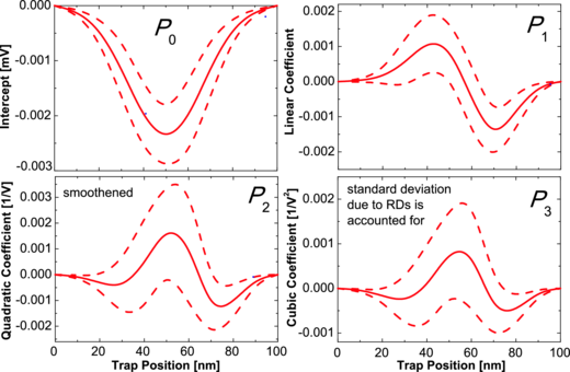
The ΔV th(V d) characteristics simulated using our compact model for different XT are shown in Figure 5.10. These
curves exhibit similar behaviour to their counterparts simulated with TCAD for different XT, and can be well fitted with
cubic polynomials. Moreover, the analytical approach allows us to understand the origin of this behaviour. For example, the
threshold voltage shift induced by a trap in the middle of the channel is the largest. This is fully consistent with the results
from Figure 5.9 which state that the impact of such traps is equivalent to a concentration shift increase by several orders of
magnitude. Furthermore, this agrees with previous literature reports [10, 53, 54]. The sign of the ΔV th(V d) dependence
(i.e. slope P1) is explained by the interplay between the two contributions. On the one hand, at lower V d the magnitude of
the threshold voltage shift should be lower which originates from the behaviour of Id-V g characteristics versus V d
(Figure 5.9(inset)). However, this is relevant only if the drain bias dependence of the concentration peak is not
significant, which is the case for traps situated at the source side of the channel (Figure 5.9(left)). Therefore, a
positive slope P1 is obvious for these traps. On the other hand, for traps situated closer to the drain, the
contribution introduced by the abrupt decrease of the concentration shift at larger V d (Figure 5.9(right)) is
more pronounced, making the values of P1 negative. In the middle of the channel both contributions nearly
compensate each other and therefore the linear term in ΔV th(V d) dependence is small (i.e. P1 changes sign).
The results provided in Figure 5.10(right) show that the model allows for a reasonable reproduction of the
fluctuations introduced by random dopants. This means that our compact model can be applied to simulate the
reference data for the trap location technique, which would allow for the avoidance of time-consuming TCAD
simulations.
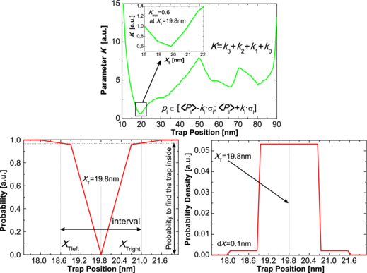
Figure 5.12: Illustration of the working principle of our trap location algorithm for XT=20nm. The proximity of
the experimental ΔV th(V d) to the mean curve simulated using TCAD or the compact model is determined by the
parameter K. A typical K(XT) dependence shows that Kmin is observed at XT=19.8nm, which is the most likely
extracted lateral defect position. The probability of finding the trap inside several intervals around an extracted
XT is equivalent to the probability with which the points XTleft, XT and XTright can be separated with respect to
the narrowest intervals [⟨Pi⟩-kiσi; ⟨Pi⟩+kiσi] selected at each point. The probability density corresponding to the
interval dX=0.1nm presents a distribution around XT, which originates from the uncertainity introduced by the
random dopants.
5.5 Extraction of the Lateral Trap Position
5.5.1 Method Description and Verification
The results provided above introduce the concept of our trap location technique, which is based on the observation that the
impact of the lateral trap position XT on the shape of ΔV th(V d) curves is typically stronger than the fluctuations induced
by random dopants. Thus in order to extract the lateral trap position from the experimental data, we parameterize the
results of the TCAD simulations using a cubic polynomial function ΔV th(V d)=∑
iPiV di and determine the coefficients P
i
for each random dopant configuration corresponding to a certain XT. The mean TCAD coefficients ⟨Pi⟩ and ⟨Pi⟩±σi, with
σi being the standard deviations induced by the random dopants, are subsequently calculated. Their dependences on the
lateral defect position are shown in Figure 5.11. Note that although in the simulations XT has been varied using 10nm
steps, the values of Pi have been then interpolated at all intermediate XT points using 0.1nm steps. The
lateral trap position was evaluated according to an algorithm which compares the cubic parameterization
coefficients pi, obtained from the experimental data (e.g. Figure 5.2) to those Pi which have been simulated using
TCAD.
The working principle of our trap location technique is illustrated in Figure 5.12. For each XT one can find a minimum
ki which guarantees that pi lies inside the interval [⟨Pi⟩-kiσi; ⟨Pi⟩+kiσi]. Therefore, the proximity between experimental
and TCAD data will be reflected by the sum K=∑
iki. The parameter K is a function of the lateral defect
coordinate XT which reaches its minimum value when the combination of pi lies closest to the corresponding ⟨Pi⟩
(Figure 5.12(top)). Since it is supposed that the ΔV th(V d) curve obtained from TDDS measurements is associated
with an individual defect, the corresponding value of XT is considered the most likely lateral position of this
defect.
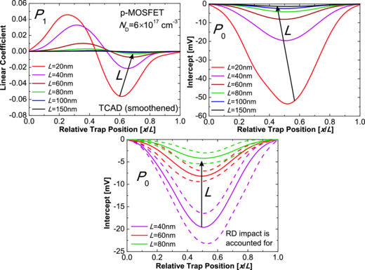
Figure 5.13: The dependences of the slope and the intercept of the ΔV th(V d) characteristics on XT simulated
with TCAD for devices with different channel lengths. Clearly, for smaller L the impact of the lateral trap position
on the magnitude and drain bias dependence of ΔV th increases more significantly than the magnitude of random
dopant fluctuations (bottom plot). Therefore, although in ultra-scaled devices the impact of random dopants is more
pronounced [9], device scaling will even lead to an improvement in the accuracy of our trap location technique.
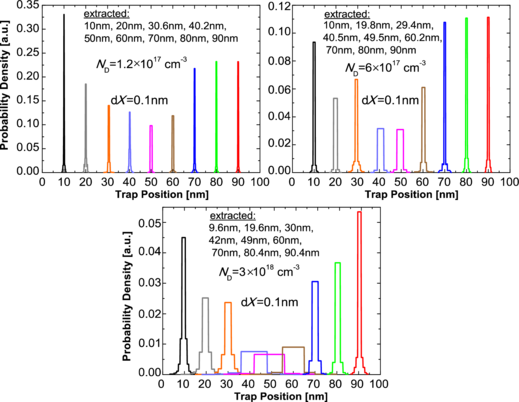
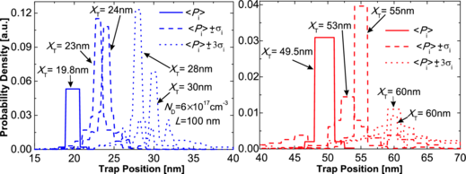
Figure 5.14: The probability densities obtained for similar MOSFETs with L=100nm and three different channel
doping levels. The algorithm is applied to the ΔV th(V d) characteristic closest to the mean TCAD curve. Therefore,
the results reflect the best accuracy which can be achieved with our trap location technique for different sections of
the device channel (benchmark XT is varied between 10nm and 90nm using 10nm steps). In all cases the impact of
random dopants is stronger in the middle of the channel. The best overall accuracy is reached for the device with
the lowest ND.
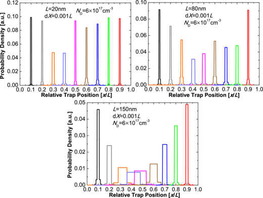
Figure 5.15: The probability densities obtained for similar MOSFETs with ND=6 × 1017cm-3 and three different
channel lengths. Similarly to Figure 5.14, the algorithm is applied to the ΔV th(V d) characteristic which is closest to
the mean TCAD curve, while the benchmark trap position is varied in 0.1L steps. Also, a small interval dX=0.001L
is used to calculate the probability density. Clearly, the best overall accuracy is reached for the device with the
smallest L.
After the lateral defect position is evaluated, the probability that all four intervals [⟨Pi⟩-kiσi; ⟨Pi⟩+kiσi] obtained for the
extracted XT do not simultaneously overlap with their counterparts for neighboring points, XTleft and XTright, is determined.
This probability is interpreted as the probability that the trap is situated inside the interval [XTleft, XTright] centered at the
extracted XT (Figure 5.12(bottom)). Then, the obtained probability can be replotted in terms of a normalized density,
which is calculated for each XT and dX as a probability to find the trap inside the fixed interval [XT-dX; XT+dX]. Note
that the consideration of all four coefficients results in high accuracy of the lateral trap position evaluation. This
is because the proximity of the experimental coefficients to their TCAD counterparts is determined more
reliably. Thus the neighbouring points can be separated with a higher probability, which increases the spatial
resolution.
As follows from the above description, the accuracy of our trap location technique depends on the impact of the random
dopants on the shape of ΔV th(V d). Since the impact of random dopants is known to be stronger in devices with smaller
L [9], one could expect the method to not allow an accurate extraction of XT in ultra-scaled devices. However, the results of
our TCAD simulations (Figure 5.13) show that the magnitude and drain bias dependence of ΔV th are considerably more
sensitive to XT if a device with smaller L is considered. Moreover, the increase in the magnitude of the ΔV th(V d) versus XT
dependence is stronger compared to the increase in the magnitude of the random dopant fluctuations. This will lead to an
even higher precision for ultra-scaled devices. Therefore, below we operate with a relative accuracy given as a percentage of
L.
In order to verify the correct functionality of the described trap location technique, we check if the reverse algorithm
reproduces the benchmark XT. For this purpose we select one of the ΔV th(V d) curves simulated by TCAD for a certain
configuration of random dopants. Initially, we examine the curve which is closest to the mean for the considered benchmark
XT. This characteristic is used as experimental data for our algorithm. In this way, the optimum accuracy of the method can
be evaluated. The procedure has been repeated for numerous lateral defect coordinates along the channel. First we examined
devices with different channel doping levels ND and L=100nm. The obtained results, plotted in terms of
probability densities, are given in Figure 5.14. In all cases the error in the extracted XT rarely exceeds 2% of L.
However, for the traps located near the middle of the channel, the distributions are broader and their heights
lower. This is because the fluctuations of ΔV th induced by random dopants are more significant [27]. The
observed behaviour of the probability density can be well described by a Gaussian distribution. The reason
for a small deviation is that the precision of the algoritm is limited by several percents of L, especially in
the middle of the channel. Another important feature is that the accuracy of our technique decreases with
increasing channel doping. This originates from a weaker ΔV th(V d) dependence observed for devices with
high ND. Therefore, the impact of random dopants is more pronounced, which leads to a broadening of the
distributions.
As a further verification step we attempt to capture the impact of the channel length on the accuracy of our technique by
performing a similar procedure for the devices with ND=6 × 1017cm-3 and different L. For a more detailed comparison, in all
cases the lateral trap position is varied in 0.1L steps, while the probability density is calculated using a small interval
dX=0.001L. The obtained results are shown in Figure 5.15. Clearly, the best accuracy is reached for the device with the
smallest L=20nm, while for its counterpart with L=150nm the technique is significantly less accurate. This is because the
ΔV th(V d) dependence becomes significantly stronger for ultra-scaled devices, while the impact of random dopants increases
only marginally (cf. Figure 5.13). Also, for the central traps the accuracy is more sensitive to variations of
L.
Finally, we examine the device with L=100nm and ND=6 × 1017cm-3 and repeat the procedure with characteristics
which strongly deviate from the mean. In such a case the ΔV th(V d) curves are considerably displaced from
the mean curve, i.e. the deviation of the parameterization coefficients from ⟨Pi⟩ is stronger. The obtained
probability density distributions are plotted in Figure 5.16. They correspond to border traps situated at
XT=20nm (left) and XT=50nm (right). The ΔV th(V d) characteristics with Pi=⟨Pi⟩±σi and ⟨Pi⟩±3σi were
examined. One can see that the uncertainty in the extracted lateral trap position for coefficients spread within
[⟨Pi⟩-σi, ⟨Pi⟩+σi], which is the most common for the considered devices, does not exceed 5%. For the case
of an extremely strong impact of random dopants, when the ΔV th(V d) shape strongly deviates from the
mean (i.e. [⟨Pi⟩-3σi, ⟨Pi⟩+3σi]), the error rarely exceeds 10%, even if the trap is situated in the middle of
the channel. This is still better than our knowledge about technological parameters of the transistors, such
as doping profiles, and thus sufficient for the practical application of our method to characterize industrial
MOSFETs.
5.5.2 Simplified Technique
The use of TCAD allows for the simulation of the reference data for the trap location technique with rather high accuracy.
However, the technique requires substantial computational resources. Therefore, initially we attempted to reproduce the
observed behaviour of the ΔV th(V d) curves for different XT using a compact model described above. In the next
step we found an even more efficient way to simplify our trap location algorithm without a significant loss of
accuracy.
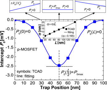
This further simplification of our technique is based on the realization that the main information regarding the lateral
trap coordinate is given by the slope P1 and the intercept P0 of the ΔV th(V d) curve. The sign of the former
determines whether the trap is at the source or at the drain side of the channel and the magnitude of the latter is
responsible for the proximity of the trap to one of the electrodes. Knowing that the mean dependence of P0
on the lateral trap position XT has a universal shape which is symmetric with respect to the middle of the
channel (e.g. our simulations (Figure 5.11) or Refs. [10, 27]), we can approximate it using a Gaussian function
(Figure 5.17):
 | (5.4) |
where it is assumed that P0max=P0(XT=L∕2) and P0(XT=0)=P0(XT=L)=0. Based on TCAD simulations performed
for devices with different L, the standard deviation σ is found to be proportional to the channel length L
as σ=αL with α≈0.17 (Figure 5.17, inset). Therefore, the relative lateral trap position can be estimated
by
 | (5.5) |
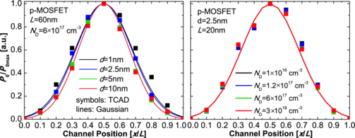
Interestingly, the gate oxide thickness d and channel doping ND mainly impact the values of P0max which have to be
determined experimentally. At the same time, the parameter α is almost independent of these quantities
(Figure 5.18).
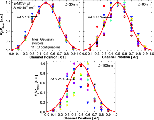
However, an exact Gaussian fitting of the P0(XT) dependence is possible only for the case P0=⟨P0⟩±nσ0 with σ0 being a
standard deviation and n constant along the channel. In reality, for each channel coordinate the values of P0 can be
randomly distributed within the interval [⟨P0⟩-3σ0; ⟨P0⟩+3σ0] due to the impact of random dopants. Therefore, for some
configurations of random dopants, the shape of the P0(XT) dependences may deviate from a Gaussian, thus
introducing some uncertainty. In Figure 5.19 it is illustrated that this uncertainty δX decreases from below
25% for L=100nm to below 5% for L=20nm. This is because the increase of the magnitude and coordinate
dependence of P0 for devices with smaller L is more significant than the increase of the magnitude of the random
dopant fluctuations (cf. Figure 5.13). Therefore, our simplified technique is even more suitable for ultra-scaled
devices.
One should note that the exact point at which P1 changes its sign is also affected by the random dopants and can deviate
within 5% from the middle of the channel (cf. Figure 5.11). This may lead to a wrong determination of the channel side at
which the trap is situated, but only for central traps. Therefore, some additional uncertainty of around 10% has to be
expected for these traps.
The input data necessary to estimate the lateral trap position XT using equation 5.5 can easily be extracted from the
experimental results. The value of P0max is determined only once for each device from the ΔV th(V d) characteristic
corresponding to the middle of the channel (XT=L∕2). This curve typically has a near-zero slope P1 and the largest among
all other values for the intercept P0; therefore it can easily be discerned. Knowing the value of P0max, one can analyze all
other ΔV th(V d) curves from the considered dataset in order to extract P0 and sign(P1) (Figure 5.17(top)) and then apply
equation 5.5 to estimate XT.
The necessary condition for the successful application of the simplified version of our trap location technique is
to have at least one ΔV th(V d) curve corresponding to XT=L∕2 within the experimental dataset (i.e. with
P0=P0max and P1=0). However, taking into account that modern nanoscale MOSFETs may contain only a
limited number of defects [90], one can imagine a situation when such a curve is not available. In particular,
this is the case for our experimental dataset provided in Figure 5.2. In such a case one can perform a visual
analysis of all measured ΔV th(V d) curves in order to find the one which corresponds to the trap situated closest
to the middle of the channel. Such a curve will have the largest P0 and at the same time the smallest P1.
In the case of Figure 5.2, this will be trap A5. Then, this ΔV th(V d) curve must be used to determine the
value of P0max, which allows us to extract the positions of all other traps using equation 5.5. Although some
additional inaccuracy may be introduced, it will not be significant for the case where the reference curve used to
extract P0max corresponds to a trap situated not very far from the middle of the channel. Also, one should
note that in a particular situation of Figure 5.2 the trap A3 could also be used as a reference to extract P0.
However, the universality of equation 5.5 requires the selection of the trap which has a maximum intercept
P0.
Alternatively, one can perform a visual qualitative analysis of the experimental traces (e.g. Figure 5.2) and immediately
recognize the ΔV th(V d) curves which correspond to traps situated at the source side (P1>0) and the drain side (P1<0) of
the channel. Moreover, traps with a larger P0 are situated closer to the middle of the channel while those with a smaller P0
are closer to the contact regions.
5.5.3 Results and Discussions
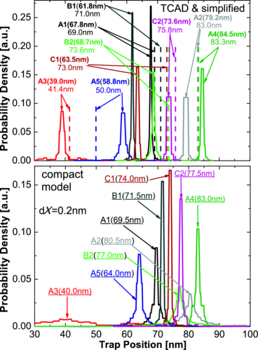
We have applied our trap location technique to the experimental results given in Figure 5.2 (p-MOSFET, L≈100nm,
ND ≈6 × 1017cm-3) and extracted the positions of all nine detected individual traps. First, we employed the results of our
TCAD simulations as a reference. The obtained probability density distributions are plotted in Figure 5.20(top). The results
show that the traps can be located with a rather high accuracy inside narrow intervals. The width of these intervals is
typically related to the impact of the random dopants. For this reason, the obtained distributions are broader for traps close
to the middle of the channel where the device is more sensitive to random dopants. In the same plot, the
values of XT estimated using our simplified trap location method (equation 5.5) are given. The value of
P0max has been estimated from the ΔV th(V d) curve corresponding to the trap A5 which is the closest to
XT=L∕2. Although the simplified technique does not allow for any probability calculations and leads to a
single value of XT, the results are very similar to those obtained using TCAD data. The typical difference
in the extracted XT values in all cases is below 10% of the channel length, while accuracy is expected to
improve for smaller devices. Therefore, taking into account that the TCAD simulations require several weeks of
cluster simulations and that the simplified algorithm gives the results in several minutes, we conclude that the
substitution of the precise algorithm with the simplified one is quite appropriate if one needs to increase
efficiency.
Another possibility to simplify the entire trap location procedure is to replace the TCAD simulations by the compact
model in our general algorithm (Figure 5.20(bottom)). However, this still requires some computational resources, while the
results are typically similar to those obtained using the simplified technique. Therefore, we conclude that the use
of the compact model is reasonable mostly for the physical interpretation of the TCAD and experimental
results.
Finally, we remark that although the entire above description is based on the results obtained for p-MOSFETs, it is
obvious that our trap location technique can be used for n-MOSFETs as well. The main point to note is that in the case of
n-MOSFETs, ΔV th is positive. However, the dependences of the parameterization coefficients of ΔV th(V d) curves versus XT
are similar to those observed for p-MOSFETs.
5.6 Chapter Conclusions
We have presented a detailed analysis of the impact of charged single defects on the performance of modern nanoscale
MOSFETs. Based on the obtained results a precise method for the extraction of the lateral position of traps
in nanoscale MOSFETs has been suggested. The main advantage of our technique compared to the ones
reported previously is that it fully accounts for the impact of random dopants. Our approach exploits the fact
that the slope and curvature of the trap-induced threshold voltage shift versus drain bias of a single trap is
considerably less sensitive to the random dopants as opposed to the lateral trap position. Therefore, we have
demonstrated that the lateral defect coordinate can be estimated with a precision of several percents of the channel
length. In addition, we have proposed a compact model that allows for the capture of the essence of the impact
of charged trap on the device performance and is also suitable for calculation of the reference data for the
algorithm without running time-consuming TCAD simulations. Moreover, we have introduced a simple expression
which allows for the estimation of the lateral trap position directly from the experimental data and have
demonstrated that the extraction uncertainty decreases for devices with smaller channel length. Therefore, the
simplified version of our trap location technique allows us to avoid both time-consuming TCAD simulations
and the compact model. This considerably increases the efficiency of the entire procedure. Finally, we have
demonstrated the applicability of all modifications of our trap location technique using experimental TDDS
data.