Chapter 6
Reliability of Graphene FETs
Miniaturization of modern MOSFETs with simultaneous improvement of their performance presents a crucial problem for
modern microelectronics. Searching for a solution to this problem creates a high demand for next-generation channel
materials capable of being used as alternatives to Silicon. In the meantime, special attention is being paid to 2D materials
capable of maintaining both a decrease in the dimensions and improvement in the main characteristics of industrial
MOSFETs. Within these materials, graphene has attracted the most considerable amount of attention. This
is due to its unique physical and electrical properties, such as an extremely high room-temperature carrier
mobility [50, 133] and a high saturation velocity [36]. Moreover, graphene is remarkably compatible with standard CMOS
technology [177]. This is especially important for enhancement of the performance and functionality of advanced
microelectronic devices and, consequently, silicon integrated circuits. At the same time, practical realization of
devices based on any new material creates a demand for characterization of their reliability. Therefore, this
chapter is devoted to the investigation of the reliability of graphene FETs. Similarly to the case of Si MOSFETs
described above, this study will be associated with the analysis of the impact of charged traps on device
performance. However, the typical dimensions of graphene field effect transistors (GFETs) are still in the
micrometer range, while the technology of their fabrication is still far below Si standards. Hence, reliability of these
devices is determined by the impact of continuously distributed charged traps rather than single discrete
defects.
6.1 Introduction
Since the discovery of graphene in 2004 [133], many successful attempts at fabricating GFETs [108, 112, 127, 126, 74, 40]
and related electronic devices [176, 192] have been undertaken. Beyond such demonstrations of device functionality for
potential applications, process integration issues, such as low resistance electrical contacts and reliable dielectric interfaces
with graphene, are urgent topics requiring further research to assess the true potential of graphene technology.
In particular, a rigorous method for the quantification of dielectric quality and reliability in terms of the
charged trap density is needed. Few attempts have been made to try to describe dielectric reliability in terms of
bias-temperature instability (BTI) [82, 113, 116, 117], one of the key figures of merit for reliability in Si
MOSFETs [80, 7]. However, despite significant advances in the overall understanding of GFET reliability, none
of these works reports a systematic method to benchmark BTI dynamics in GFETs. Also, no analysis has
been attempted with respect to hot-carrier degradation (HCD), which is another key reliability issue in Si
MOSFETs [171].
In the course of this work we perform a detailed study of both BTI and HCD on the high-k top gate of double-gated
GFETs and compare the dynamics of these phenomena. We demonstrate that despite the defect densities measured for
GFETs are still considerably larger than those known from Si technologies, the dynamics of BTI are in general
comparable. This allows us to understand BTI in GFETs using standard methods previously developed for Si
technologies if the degradation dynamics are expressed in terms of a Dirac point voltage shift as opposed to an
ill-defined threshold voltage shift. Moreover, for some stress conditions HCD in GFETs can also be benchmarked
using the same methods which allows for quantitative estimation of the graphene/dielectric interface quality.
Also, we compare the BTI dynamics on the high-k top gate and SiO2 back gate of double-gated GFETs.
Finally, we study the impact of HCD with different polarity of HC and bias components on defect density and
mobility, and investigate the temperature dependence of the related interaction between different defects. Based
on these findings, we show that the resulting changes in the charged trap density and carrier mobility are
correlated.
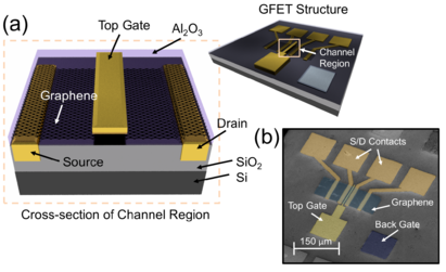
6.2 Investigated Devices: Fabrication and Basic Characteristics
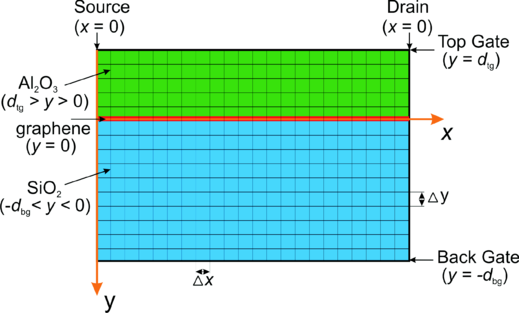
We perform our studies on double-gated GFETs with Al2O3 as a top gate insulator and SiO2 as a back gate insulator. The
channel length L of these devices is either 1, 2 or 4μm, while the width W can vary between 4 and 80μm. The oxide
thickness is 25nm for Al2O3 and 1800nm for SiO2. However, in some devices 92nm thick back gate oxide was used, which
allowed us to observe back gate BTI at reasonable stress voltages. An isometric view and a schematic cross-section of the
devices used as test benches are given in Figure 6.1.
The GFETs were fabricated at the group of Prof. Max Lemme on thermally oxidized silicon chips with a
given silicon dioxide thickness. First, a contact hole to the substrate (i.e. back gate) was etched through the
SiO2 using reactive ion etching, and subsequently filled with aluminum using thermal evaporation and a self
aligned lift-off process. Contact pads were then embedded into the SiO2 layer in order to form source and
drain contacts as well as two extra contact pads for contact and sheet resistance measurements. The contact
pads were made of gold (Au) and evaporated titanium (Ti) to improve adhesion to the SiO2 layer. Chemical
vapour deposited (CVD) graphene was then transferred from copper foil to the chip using a well-developed wet
graphene transfer process [177]. For this, a polymer layer was first spun onto the graphene on one side of the
copper. The graphene was etched from the other side of the copper using O2 plasma. The remaining copper
foil with graphene and polymer was then placed, copper side down, into ferric chloride. This etched away
the copper layer leaving the graphene and polymer floating on the surface. Next, the graphene was further
processed by fishing it out of the ferric chloride using a dummy wafer and placing it into a series of water and
hydrochloric acid (HCl) solutions. After cleaning, the graphene was transferred in a similar manner onto the
chip and the polymer layer was removed with chloroform. Once the graphene was transferred to the wafer,
transistor channels were structured using standard photolithography and O2 plasma. The top gate dielectric was
formed by atomic layer deposition (ALD), utilizing an evaporated aluminum seed layer of 3nm which was
oxidized to form a 5nm layer of Al2O3. A 20nm thick film of Al2O3 was then deposited on top of the seed layer
using ALD. The Al2O3 was etched using buffered hydrofluoric acid (BHF) in the areas of the contact pads.
Finally, Ti/Au top gate electrodes were deposited onto the devices using metal evaporation and a lift-off
process.
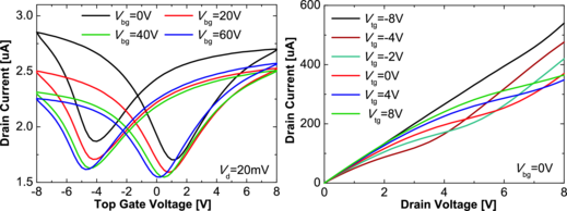
For the initial check of the device performance, we investigated the output and transfer characteristics of our GFETs.
As shown in Figure 6.2, these basic device characteristics correspond to those published previously [82]. In
particular, the top gate transfer characteristics measured at different back gate biases exhibit a modulation of
the Dirac point voltage V D by the back gate bias V bg. Also, a hysteresis related to charging/discharging of
fast oxide traps is present on the Id-V tg curves. The output characteristics measured at different top gate
biases V tg show a rather strong saturation at high drain bias V d and also exhibit some kinks for negative
V tg. The origin of the latter is associated with a change of the conductivity type in some channel regions,
which is known as ambipolar channel behaviour [125] and presents a counterpart of pinch-off behaviour in Si
MOSFETs.
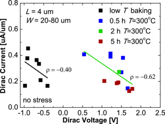
However, in our first measurements significant device-to-device variability could be observed which prevented a
systematic reliability study. This variability is determined by the distribution of the current normalized to the channel width
W and voltage values at the Dirac point. It can be described by the trend line with a certain correlation coefficient ρ
(Figure 6.3). In the spirit of the standard forming-gas anneal of Si MOSFETs [116], the devices were baked at T=300oC in a
H2/He mixture. As shown in Figure 6.3, this allowed us to obtain a significant decrease in device-to-device
variability. Namely, after baking, the distribution of the current and voltage at the Dirac point becomes narrower,
while the correlation coefficient increases. At the same time, V D is shifted towards positive values, which
suggests a change in the charged trap density. As such, this thermal treatment before electrical characterization
appears to be essential for reliability studies, which require the comparison of degradation data taken on various
devices. Also, to the best of the author’s knowledge, such small variability has so far not been reported for
GFETs.
6.3 Experimental Technique
Our experimental technique for benchmarking reliability issues in GFETs is based on the measurements of the gate transfer
characteristics, which are known to be sensitive to the detrimental impact of the environment[117, 160]. Therefore, all
measurements were performed in a vacuum (5×10⁻⁶–10-5torr).
First we studied the impact of BTI stress on the top gate transfer characteristics in order to benchmark the BTI
dynamics in GFETs. Thus, according to our technique, a constant BTI stress V tg applied on the top gate for a certain stress
time ts is followed by measuring the transfer characteristics corresponding to different recovery stages, which are measured as
a function of the relaxation time tr. Taking into account the logarithmic time dependence of the BTI degradation and
recovery, the number of experimental points used is larger within the first minutes after the stress. As will be
discussed below, we express the BTI dynamics in terms of a horizontal shift of the Dirac point ΔV D rather
than an ill-defined threshold voltage V th [113, 116, 117]. The main technical features of our method are the
following: first, the voltages V bg and V d are set to zero during stress and narrow (2–3V) V tg intervals are used
during the Id-V tg measurements. This is necessary to minimize the impact of any additional degradation
factors (e.g. hot carrier degradation). Second, the results for different stress conditions and temperatures
are obtained either on the same device or on a group of devices with negligible variability. For this reason
subsequent measurement rounds are separated by an intermediate baking step of the devices in a H2/He
mixture at T=300oC, which in most cases leads to almost complete recovery and also decreases device-to-device
variability. Third, because of large magnitudes of ΔV D, the measurements on each device are repeated using
increasing stress times ts=1, 10, 100, 1000 and 10000s while keeping V tg-V D(ts) ≈ const. The latter is necessary to
sustain an approximately constant oxide field during all experiments, making the obtained results easier to
interpret. Also, to further simplify the analysis, the gate transfer characteristics were always measured at
V d=20mV.
However, the use of V tg-V D(ts) ≈ const should be essential when the waiting time between the experiments with different
ts is not enough for a nearly complete recovery after the previous stress. In this case the difference between the sets of BTI
recovery traces measured using the stress conditions V tg(ts)=const and V tg-V D(ts) ≈ const can be significant. Conversely, if
the waiting time in between the experiments with different ts is large enough for a significant degree of recovery, the use of
just V tg(ts) ≈ const should be enough.
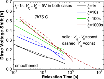
In order to compare the two stress conditions and justify our statement about the universality of using
V tg-V D(ts) ≈ const, we performed the following experiment. First, a typical set of PBTI traces was measured using
V tg(ts)=const. Next, similar measurements using V tg-V D(ts) ≈ const were performed on the same device.
The temperature T=75oC was maintained during all experiments, which in around two hours resulted in
complete recovery after the first set of measurements, even without high-temperature baking. To highlight the
difference between the two techniques, recovery after PBTI stress with a certain ts was monitored only for
10minutes.
The results given in Figure 6.4 demonstrate the difference between the two techniques which is due to incomplete
recovery on each step. A nearly complete reproducibility of the first trace is obvious because the initial stress conditions in
the two experiments were identical (i.e. V tg-V D=5V, ts=1s). However, at larger ts, the distances between the traces obtained
using the technique with V tg(ts)=const show some saturation. The reason is that in this case the resulting oxide field
(Fox=(V tg-V D)/dtg) decreases due to incomplete recovery. This is contrary to the case when V tg-V D(ts) ≈ const is
readjusted on each ts step. Another important feature which testifies to the decrease in Fox in the case of V tg(ts)=const is
that the corresponding recovery traces lie higher than for V tg-V D(ts) ≈ const. This suggests slower recovery in the
former case, which is typical for lower stress biases (note that tr=0 extrapolation is not done here). Therefore,
the use of the V tg-V D(ts) ≈ const condition makes our experimental technique universal and suitable for
application even if the recovery is rather weak. Use of this condition should allow us to avoid distortion of the
experimental results and simplify benchmarking of BTI dynamics in GFETs using general models developed for Si
technologies.
However, some of our studies require investigation of the dependence of the BTI dynamics on the stress oxide field. In
this case subsequent stress/recovery rounds with constant ts and either increasing V tg-V D and V bg=0 (top gate BTI) or
increasing V bg-V D and V tg=0 (back gate BTI) were used.
The experimental technique described above was also extended for benchmarking the dynamics of HCD in GFETs. This
was done simply by using constant non-zero V d during each of the stress rounds. However, in some cases we employed a
similar technique with a constant ts and subsequent stress/recovery rounds with increasing V d=0...±12V. This was necessary
to capture the dependence of the degradation/recovery dynamics on the magnitude of the HCD component. In the spirit
of our general technique with increasing ts, V tg-V D(V d) ≈ const and V bg=0 were maintained for all stress
rounds.
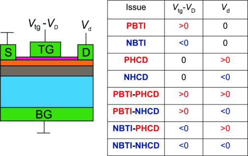
Therefore, our experimental technique allows us to study the degradation/recovery dynamics under different magnitudes
and polarities of hot carrier and bias stress contributions. Similarly to NBTI and PBTI, the impact of hot carrier
contribution with V d >0 is designated as PHCD, while its counterpart with V d <0 is called NHCD. If both hot carrier
and bias stress contribution act in conjuction, one can have NBTI-PHCD, NBTI-NHCD, PBTI-PHCD or
PBTI-NHCD. The impact of all these issues on the device performance are studied below using our experimental
technique.
6.4 Modeling of Carrier Distribution in GFET Channel
A precise modeling of carrier transport in GFETs is significantly different compared to Si technologies. This is because
graphene is a 2D material with zero bandgap and linear band edge profiles, which requires radical modifications of the
general models used in modern device simulators. Therefore, most of the literature reports provide only quite
simplified compact models, allowing for the reproduction of basic characteristics of GFETs [98, 196]. However,
interpretation of the experimental reliability characteristics requires more general information on the channel
distribution of the surface potential and carrier concentrations during the stress. In this context, implementation
of the drift-diffusion (DD) model for the case of GFETs is quite appropriate. The first attempt to adjust
generally known DD equations for GFETs was done in [4]. However, the authors of [4] consider a number of
non-trivial issues which significantly complicate the model, while at the same time are particularly important
for devices based on graphene with artificially created bandgap. On the other hand side, in [4] there is a
lack of information on the boundary conditions used, while the motivation of [4] is not linked to a reliability
study.
In the following, we provide a simple implementation of the DD model for GFETs, allowing for qualitative analysis of the
surface potential distributions and carrier concentrations under different stress conditions. At the same time, we introduce
and discuss different types of boundary conditions for carrier concentrations corresponding to different stress configurations.
This is especially important for the linking of our simulation results with the experimental reliability study of
GFETs.
The DD equations for electron and hole current densities, Jn and Jp are
 | (6.1) |
and
 | (6.2) |
where n, p, μn and μp are the electron and hole concentrations and mobilities, respectively, F and ψ are the
channel electric field and electrostatic potential, respectively, and the coordinate x expresses the position
along the graphene channel. For the diffusion coefficients Dn and Dp we use the definition from [196] which
reads
 | (6.3) |
with vF=108cm/s being the Fermi velocity in graphene and τ
tr=10ps the transport relaxation time, which determines the
carrier mean free path l=vFτtr. Contrary to a more general definition of the diffusion coefficient in graphene given in [4],
here the dependence of the diffusion coefficients on carrier concentrations is not accounted for. However, according
to our experience, this significantly improves the convergence while still leading to reasonable qualitative
results.
The corresponding continuity equations read
 | (6.4) |
and
 | (6.5) |
Here the terms on the right account for the thermal generation of carriers [4] and the equilibrium carrier concentrations
are
 | (6.6) |
According to the drift-diffusion theory, the equations above have to be solved self-consistently with the Poisson equation,
which in our case is
 | (6.7) |
Obviously, the concentration of fixed charges Df and dielectric constant ε depend on the device segment, which is
determined by the coordinate y perpendicularly to the channel.
In order to solve equations 6.4, 6.5 and 6.7, we perform their discretization using the Scharfetter-Gummel scheme [13].
The schematic layout of the meshed device is shown in Figure 6.5. The coordinate grid used in our simulations is created by
discretizing the x and y coordinates as follows:
 | (6.8) |
 | (6.9) |
 | (6.10) |
Therefore, NX+1 is the number of x points, while NYbg+1 and NYtg+1 are the numbers of y points within the back and top
gate oxides, respectively. Taking into account a significant difference in the oxide thicknesses dbg and dtg, we adjust NYbg and
NYtg so as to make the discretization step Δy=yi+1-yi constant. At the same time, the step Δx=xi+1-xi is not necessarily
equal to Δy.
Thus, the Poisson equation is discretized as follows:
 | (6.12) |
 | (6.13) |
Equations 6.11, 6.12 and 6.13 correspond to the back gate oxide, the top gate oxide and the graphene channel,
respectively. The quantities Dbg and Dtg express 2D densities of fixed charges at the graphene/SiO2 and graphene/Al2O3
interfaces. A difference compared to implementation in [4] is that we consider the full discretization of the Poisson equation
in graphene (equation 6.13) instead of using just a first order differential equation relating the electrostatics across the
channel.
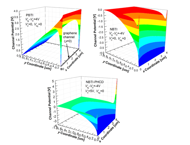
In order to solve equations 6.11, 6.12 and 6.13, we employ the following Dirichlet boundary conditions
 | (6.14) |
Therefore, we obtain the potential distribution within the graphene channel and gate oxides for various combinations of
V tg-V D, V bg and V d, i.e. different stress conditions. The simulation results for PBTI, NBTI and NBTI-PHCD shown in
Figure 6.6 look quite reasonable. However, the distributions of carrier concentrations along the channel would allow for a
more intuitive qualitative explanation of our experimental results.
We proceed with the discretization of the continuity equations 6.4 and 6.5. According to Scharfetter-Gummel scheme,
the current densities at the intermediate points are discretized as
 | (6.15) |
where B(t) = t∕(et - 1) is the Bernoulli function and x
i+1∕2 = (xi + xi+1)∕2. The index j = NYbg (i.e. graphene channel) is
skipped for simplicity. Therefore, the continuity equations read
 | (6.16) |
Obviously, solution of these equations requires boundary conditions for both carrier concentrations. However, a significant
complication compared to the case of Si technologies is that the conductivity type of the graphene channel is determined by
the applied stress rather than by the type of artificially introduced dopants. Moreover, for some combinations of gate and
drain biases the conductivity type can vary along the channel, i.e. the channel can be ambipolar [125]. In order to account
for this behaviour, we suggest two possible types of boundary conditions. Type I is used if the graphene channel is of
electron conductivity type and reads
 | (6.17) |
Type II is for the hole conductivity type of the channel and can be written as
 | (6.18) |
Therefore, the concentration of majority carriers close to the source and drain is determined by the potential difference
between graphene and the gate electrode, while its counterpart for minority carriers is calculated using the carrier balance
law.
However, equations 6.17 and 6.18 correspond to the case when the bias component is applied on the top gate of double
gated GFETs. Obviously, for back gate BTI one would get
 | (6.19) |
for Type I, and
 | (6.20) |
for Type II. Since in our case the oxide thicknesses are large enough, the impact of the quantum capacitance can be
neglected and therefore Ctg and Cbg express geometric capacitances of the top gate and back gate oxides, respectively. Also,
all the potential quantities which contribute to equations 6.17 – 6.20 are known and given by V tg-V D, V bg-V D and
V d.
As follows from the description above, in the case of the GFETs, selection of appropriate boundary conditions depends on
the polarity of applied BTI and HCD stress components. Therefore, since PBTI corresponds to the electron conduction
region of GFET, one has to use Type I boundary conditions at both electrodes. Conversely, for NBTI, Type II
boundary conditions have to be used. Activation of PHCD would lead to an additional increase of the hole
concentration close to the drain, while the NHCD component would increase the electron concentration in the
proximity of the drain. Thus in the case of PBTI-NHCD and NBTI-PHCD, the HCD component should not
change the channel conductivity type. As such, one has to use the boundary conditions of Type I and Type II,
respectively.
However, setting of the boundary conditions for PBTI-PHCD and NBTI-NHCD is more complicated, since these two
stress configurations may lead to ambipolar channel behaviour. For example, in the case of PBTI-PHCD, one should always
use Type I at the source, where the electron conductivity type is associated with the PBTI component. At the same time,
the PHCD component comes into play close to the drain. If V d is not large enough, this simply reduces the electron
concentration near the drain, while the overall electron conductivity type is conserved. Therefore, the boundary condition of
Type I has to be used at the drain as well. But a strong PHCD component can reverse the conductivity
type of graphene near the drain and make hole transport dominating. In this case the Type II boundary
condition has to be employed at the drain. Similarly, for NBTI-NCD, the boundary condition of Type II at
the source and either Type II or Type I at the drain have to be used. The former corresponds to the case
of small V d, while the latter is for large V d, leading to ambipolar behaviour. For both PBTI-PHCD and
NBTI-HNCD the transition between the different types of boundary conditions at the drain can be easily captured
empirically, since setting of a wrong type (e.g. Type I for PBTI-PHCD with large V d) always leads to unfeasible
results.
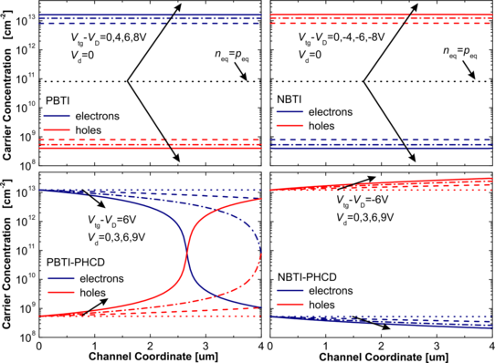
Exemplary carrier concentration profiles along the channel simulated for different stress configurations are shown in
Figure 6.7. Clearly, the concentration of both electrons and holes are nearly constant for PBTI and NBTI, while
the channel conductivity types are different. An increase of V tg-V D makes the concentration of majority
carriers larger, while reducing the amount of minority carriers. At the same time, activation of the PHCD
component acting in conjuction with NBTI increases the concentration of holes and decreases the concentration of
electrons toward the drain, making hole conductivity more pronounced. Obviously, this trend is stronger
for larger V d. If a PHCD component acts in conjuction with PBTI, the concentration of electrons, which
are the majority carriers close to the source, also decreases toward the drain. Therefore, at a certain V d the
concentration of holes at the drain side becomes larger than the concentration of electrons, i.e. the channel becomes
ambipolar.
Although implementation of graphene into the simulators allowing for the quantitative capture of the carrier trapping
dynamics remains complicated, the obtained concentration profiles are suitable for a qualitative interpretation of
the experimental results. This is because the information on the carrier concentrations in a certain channel
segment allows us to make a conclusion on whether electron or hole trapping is more favourable. Moreover, the
dependence of the carrier distributions on the magnitude and polarity of the applied stress can be qualitatively
reproduced.
6.5 Bias-Temperature Instabilities on the High-k Top Gate
The major part of our experimental studies on BTI in GFETs have been performed by applying either positive
(PBTI) or negative (NBTI) bias stress on the high-k top gate of double gated GFET. The obtained results and
their interpretation using the general models previously developed for Si MOSFETs are discussed in this
section.
6.5.1 Typical Impact on the Device Performance and Reproducibility
Based on our knowledge of GFET operation and the DD simulation results above, we can conclude that NBTI is associated
with positively charged traps, which appear as a result of hole trapping. Conversely, in the case of PBTI we are dealing with
negatively charged traps, i.e. electron trapping. Hence, the charged trap density shift ΔNT is positive for NBTI and
negative for PBTI. Obviously, any variation of NT would lead to a shift of the Dirac point voltage, which
can be expressed as ΔV D=qΔNT∕Ctg. Therefore, the simplest way to capture the impact of BTI on the
performance of GFET consists in comparison of the gate transfer characteristics measured before and after
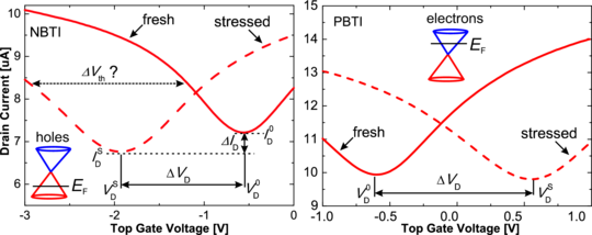
the stress. The results given in Figure 6.8 show that BTI stress results mainly in a horizontal shift of the
Dirac point voltage V D. However, some vertical drift of the characteristics ΔID is also present. The latter is
most likely related to a change in the device electrostatics and mobility, which are affected by variation of
NT.
Since Id depends on other factors (e.g. the contact resistance) and Idmax is determined by the width of the V tg interval,
the presence of ΔID makes the frequently used (but somewhat arbitrary) definition [113, 116, 117] of the threshold voltage
V th as the gate bias at which Id=(Idmax+Idmin)/2 questionable. Thus, we suggest using the Dirac point shift
ΔV D =|V D0 -V
DS|
as the main quantity for expressing GFET reliability, since it is directly linked to the variation of charged
traps ΔNT and also independent of other factors. As for the vertical shift of the Dirac point ΔID, use of this
quantity for expressing BTI degradation/recovery dynamics is also unfeasible. That is because evaluation of
the link between ΔID and ΔNT is complicated, since the vertical shift is most likely contributed by both
carrier trapping and mobility variation. Also, ΔID is impacted by contact resistance, especially if ΔV D is
large.
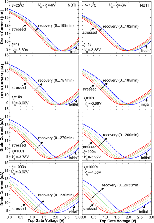
Experimental results illustrating the time evolution of transfer characteristics during and after NBTI stress at T=25oC
and T=75oC are shown in Figure 6.9. As expected, a longer NBTI stress causes a stronger shift of ΔV
D towards more
negative voltages. Also, significant drifts are recorded even at very low stress biases, corresponding to about 1MV/cm
(compare to the typically used 4 – 8MV/cm stress in Si technologies). During the recovery, ΔV D returns
back to its initial position which happens faster at a higher temperature. We thus can extract V D for each of
the measured characteristics and obtain the recovery traces versus the relaxation time. Analysis is provided
below.
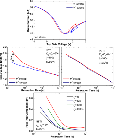
The transfer characteristics shown in Figure 6.9 were measured by sweeping V tg from positive to negative values (V -
sweep mode). However, it has been observed that when the measurements are performed from negative to
positive V tg (V + sweep mode), the initial NBTI degradation is more severe, which is due to charging of fast
traps during the stress. The fast trap component associated with these defects is also responsible for the
pronounced hysteresis and becomes stronger for larger ΔV D, while recovering within about 100s (Figure 6.10).
However, contrary to NBTI, the magnitude and recovery of PBTI degradation are independent of the sweep
direction.
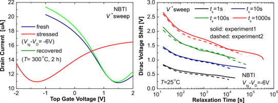
Figure 6.11(left) illustrates that high-temperature baking at 300oC for 2hours leads to a nearly complete recovery
of NBTI degradation. This allows us to minimize the impact of device-to-device variations by performing
numerous measurements on the same device. In Figure 6.11 (right) one can see the two sets of recovery traces
measured for the same device at T=25oC, with an intermediate baking step at T=300oC for 2hours. The
results are well reproducible, despite the presence of both fast and slower trap components. Therefore, the
reliability characteristics measured on the same device using different stress conditions should be easier to
interpret.
6.5.2 Temperature Dependence and Fitting with CET Map and Universal Models
The fast trap component observed when monitoring the NBTI recovery using the V + sweep mode makes the interpretation
of the resulting ΔV D recovery traces more complicated. Moreover, the slow long-term degradation/recovery dynamics are
more suitable for comparison with Si technologies than the hysteresis behaviour. Therefore, the results measured using the
V - sweep mode (e.g. Figure 6.9) will be analyzed in detail below.
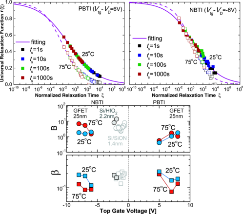
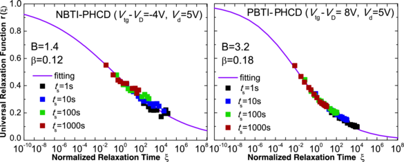
First we attempt to fit the ΔV D recovery traces measured without the fast trap component using the universal
relaxation relation previously developed for Si technologies [61, 64]. As has been discussed in Section 3.2, this
universal relation reads r(ξ) = 1∕(1 + Bξβ) with the normalized relaxation time ξ = t
r∕ts and empirical fitting
parameters B and β. In Figure 6.12 we show that perfect fits can be obtained for both PBTI and NBTI at
T=25oC and T=75oC. Moreover, the parameters B and β employed for fitting are very similar to those obtained
from Si data, confirming the similarity in the underlying physical degradation processes. However, contrary
to Si technologies, no permanent (‘dangling bond’) component needs to be taken into account during the
extraction.
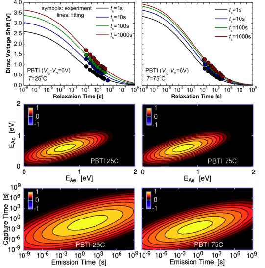
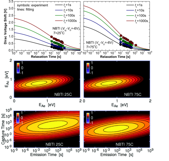
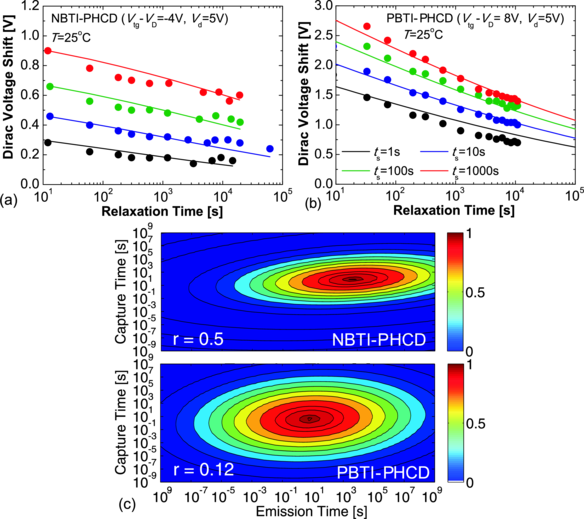
For a final comparison with Si technologies, we show that the obtained recovery traces can be fitted with the
capture/emission time (CET) map model [69] for both PBTI and NBTI. The CET map model assumes that BTI is the
collective response of independent defects which exchange charges with the channel, each following a first-order non-radiative
multiphonon process. Confirmed by extensive Si datasets, the essential ingredients of the model are the widely distributed,
correlated, and temperature dependent capture and emission times. These quantities can be well described
using bivariate Gaussian distributions of the respective activation energies. The sets of experimental ΔV D
recovery traces fitted with the simulation results, and corresponding CET map distributions are given in
Figure 6.13 and Figure 6.14 for PBTI and NBTI, respectively. In both cases the same absolute value of
V tg-V D and two different temperatures (T=25oC and T=75oC) were used. The typical initial values of the
charged trap density shift ΔNT for GFETs are around 1012cm-2 which is still considerably larger than for Si
technologies.
In our first studies the measurements were performed without an intermediate high-temperature baking/recovery step.
Therefore we had to investigate the BTI dynamics for various stress conditions on different devices. In that case
simultaneous fits of data for different stress conditions were often difficult to obtain because of the detrimental effects
of variability (cf. Figure 6.3) which are not considered in the CET map model. However, the experimental
results measured on the same devices (Figures 6.13 – 6.14) are fully consistent with the theory. Similarly to
Si technologies, for both PBTI and NBTI the degradation is stronger and recovery is faster at higher T.
Also, the dependence of the degradation magnitude on stress time is well reproduced. Finally, the obtained
CET distributions for activation energies and time constants are very similar to the ones extracted for Si
MOSFETs [69]. This means that the degradation/recovery dynamics of BTI in GFETs and Si technologies are very
similar.
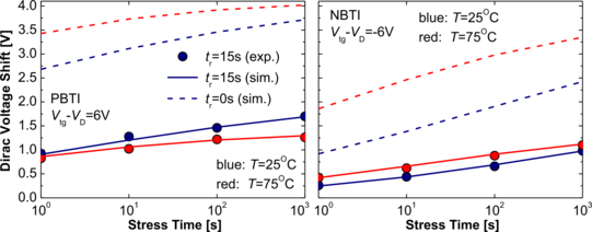
In some cases, as a consequence of the relatively large measurement delay caused by the full Id-V tg sweeps, the
degradation appears to be lower at higher T, in agreement with previous results [113, 117]. However, in Figure 6.15 we
show that the measurement delay can be extrapolated to tr≈0 using the CET map model. The values of ΔV D(tr≈0)
obtained for T=75oC are always larger than their counterparts for T=25oC. This confirms that a lower degradation at higher
temperature is an artefact, which appears due to a significant measurement delay and faster recovery at T=75oC. This
artefact is typically more pronounced for PBTI than for NBTI because the recovery of PBTI is faster, especially at higher
temperatures.
In Si technologies, two Gaussian distributions have to be used to describe the NBTI recovery data [161, 57]. The first
dominates the experimentally observed recovery and has mean activation energies for capture and emission slightly below
1eV, just like our GFETs. The second distribution has mean activation energies at about 1.5eV/2eV for capture and
emission, respectively. This second distribution has been tentatively assigned to dangling bonds (Pb centers)
which are responsible for the permanent component. Interestingly, this distribution is absent in our graphene
transistors, which is consistent with the Van der Waals bonding between graphene and Al2O3. Nevertheless, we can
conclude that the CET map model established for Si MOSFETs can be successfully applied to GFETs as
well.
Overall, we can conclude that our BTI assessment methodology based on the models used for Si technologies is suitable
for quantifying the quality and reliability of GFETs and graphene/dielectric interfaces in general. This is because the BTI
degradation/recovery dynamics in GFETs and Si MOSFETs are similar despite the absence of dangling bonds and larger
defect density shifts in the former case.
6.6 Bias-Temperature Instabilities on the SiO2 Back Gate
Although in the course of this work we have mostly dealt with BTI on the high-k top gate, some BTI measurements on the
SiO2 back gate were also performed. However, investigation of the back gate BTI on our standard devices was
not possible, since no visible degradation of the 1800nm thick back gate oxide could be caused using stress
voltages below 100V. Therefore, similar devices with 92nm thick SiO2 layers have been fabricated, allowing us
to observe back gate BTI at reasonable stress voltages. The results obtained on these devices are discussed
below.
6.6.1 Stress Oxide Field Dependence and Recovery
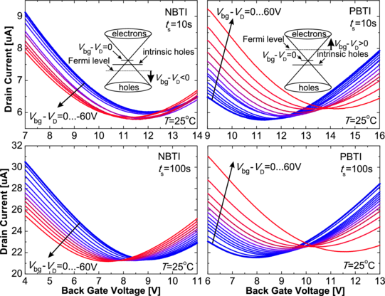
In Figure 6.16 we show the measured evolution of the back gate transfer characteristics after subsequent NBTI and PBTI
stresses with V bg-V D varied from 0 to ±60V in ±5V steps. Clearly, the typical impact of BTI is similar to what is observed
on the high-k top gate. Therefore, we express the degradation magnitude in terms of a Dirac point voltage shift
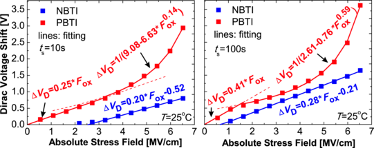
ΔV D = qΔNT/Cbg. The resulting dependences of ΔV D on the stress oxide field Fox=(V bg-V D)/dbg are plotted in
Figure 6.17 for the stress times ts = 10s and ts = 100s. Contrary to Si technologies, in both cases PBTI degradation is
stronger than its NBTI counterpart. Moreover, there is a significant difference between PBTI and NBTI with respect to the
dependence of the observed Dirac voltage shifts on the stress oxide field. While the NBTI shift linearly increases
versus Fox, growth of the PBTI shift is linear only at small Fox and can be fitted with a Langmuir power
law f(x) = 1∕(a -bxc) at larger oxide fields. At the same time, for both NBTI and PBTI the slopes in the
linear regions increase versus ts. This is because the probability of carrier trapping becomes larger for longer
stresses.
Interestingly, transition of PBTI curves to a Langmuir-like behaviour takes place at smaller Fox if ts is larger. This
leads to a smaller difference between PBTI and NBTI shifts at moderate ts, although PBTI still remains
stronger than NBTI (Figure 6.17(right)). Since in GFETs PBTI is associated with electron trapping and
NBTI is due to hole trapping, we assume that the main reason for the observed behaviour is the difference
in the kinetics of the two processes as well as the energetic alignment of the defect bands with the Fermi
level in the graphene channel. Another issue which contributes to the asymmetry between NBTI and PBTI
is the positive initial values of V D, which are typical for all our GFETs. This means that our graphene is
p-doped, i.e. some intrinsic holes are present even if V bg = 0. Most likely, trapping of these intrinsic holes is
less efficient, especially if the stress time is small. Therefore, NBTI degradation is weak at small Fox, when
-V D < V bg -V D < 0, i.e. the applied voltage is not enough to shift the Fermi level below the intrinsic level
(Figure 6.16(inset)).
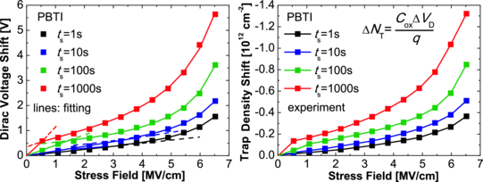
Contrary to NBTI, PBTI is independent of the intrinsic hole level position, since any stress with V bg -V D > 0
introduces extrinsic electrons and shifts the Fermi level into the conduction band. This is why some PBTI degradation is
clearly visible even after a stress with ts = 1s and Fox < 1MV∕cm (Figure 6.18(left)). However, the dependence of the
magnitude of the PBTI shifts on the stress oxide field is strongly correlated with the stress time. For example, if ts is small,
the PBTI shift moderately increases in a linear manner up to a quite large Fox. Conversely, in the case of long
stresses, a strong linear dependence of ΔV D on Fox is observed only in a very narrow range of small Fox, and is
immediately substituted by a Langmuir-like behaviour. Obviously, the same type of oxide field dependence is typical
for the charged trap density shift ΔNT, which is proportional to ΔV D (Figure 6.18(right)). However, the
values of ΔNT observed for GFETs are 1011–1012cm-2, which is significantly larger than for Si technologies
(1010–1011cm-2) [59].
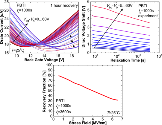
Next we examine the time evolution of the back gate transfer characteristics after the PBTI stress. In order to do so, we
fix a comparably large ts = 1000s and monitor recovery during the one hour after the end of stress with a certain V bg-V D.
The time evolution of the transfer characteristics and resulting ΔV D(tr) recovery traces are shown in Figure 6.19. Clearly,
the back gate BTI degradation in GFETs is recoverable, similarly to its counterpart observed on the high-k top
gate and also for Si technologies [76, 151, 158]. Remarkably, after the stress with smaller oxide field, the
recovery is faster, while the fraction of recovered degradation is larger (Figure 6.19, bottom). The latter
observation is also similar to Si technologies [158]. At the same time, the distances between the recovery traces
increase versus V bg-V D, following the Langmuir-like dependence which is typical for PBTI with ts = 1000s (cf.
Figure 6.18).
6.6.2 Comparison with Top Gate BTI
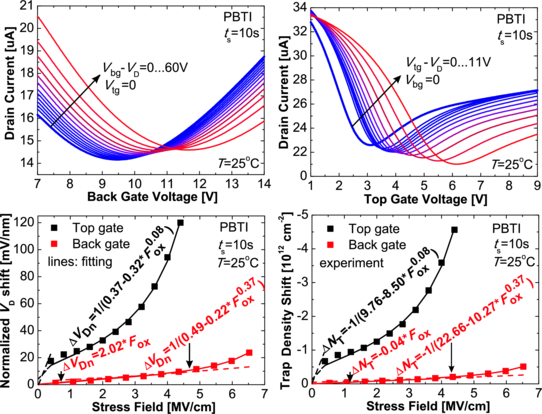
In Figure 6.20 we compare the results for PBTI degradation obtained on the SiO2 back gate and Al2O3 top gate of the
same GFET. Clearly, the direction of the Dirac point voltage shift is the same, which means that electron
trapping takes place independently of whether the PBTI stress is applied on the top or back gate of GFET. At
the same time, the Dirac point current is shifted in opposite directions, which is most likely because the
negatively charged traps situated in SiO2 and Al2O3 interfacial layers impact the carrier mobility in a different
manner.
However, the significant difference in the oxide thicknesses requires us to operate with a normalized Dirac point voltage shift
ΔV Dn = ΔV D∕dox (cf. [148])
when making a quantitative comparison of the degradation magnitudes on the top and back gates. As shown in Figure 6.20,
the magnitude of PBTI degradation on the top gate is considerably larger. This is similar to Si technologies, where the
reliability of high-k oxides also presents an important issue [149]. At the same time, the dependence on Fox in the case of
top gate PBTI is purely Langmuir-like, while an abrupt linear increase is expected only close to Fox = 0 so as to maintain
zero degradation at zero oxide field. This is despite ts = 10s, which leads to a significant linear region in the case of
back gate PBTI. In other words, the behaviour of the top gate PBTI degradation versus Fox observed using
ts = 10s is similar to those which has been measured on the back gate with significantly larger stress times
(Figure 6.17). Also, the resulting charged trap density shift is larger for the top gate PBTI. Therefore, we
can conclude that the high-k top gate is considerably less stable with respect to BTI than the SiO2 back
gate.
To conclude, we have shown that there is a considerable asymmetry between back gate NBTI and PBTI in terms of
degradation magnitude and its dependence on the stress parameters. At the same time, the recovery of the back gate BTI
has been shown to be similar to those previously reported for Si technologies and for the high-k top gate BTI in GFETs.
Finally, the back gate BTI degradation dynamics are similar to those observed on the high-k top gate, although the
magnitude in the latter is significantly larger. Therefore, we can conclude that the BTI stability of the SiO2 back gate is
better compared to the high-k top gate.
6.7 Hot-Carrier Degradation
The results discussed in the previous sections allowed us to understand the degradation/recovery dynamics of BTI in
GFETs. However, in real device operation conditions, a non-zero drain bias is typically applied. Therefore, an additional
degradation due to the impact of hot carriers is expected. In this section we discuss the results of the HCD dynamics
obtained on the high-k top gate of similar double-gated GFETs.
6.7.1 First Observations and Typical Impact on the Device Performance
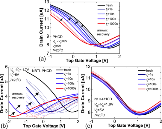
In order to observe HCD in GFETs and obtain an initial understanding of its dynamics, we have performed measurements
using a fixed V d=5V (i.e. PHCD) and three different V tg-V D corresponding to NBTI (V tg-V D<0), a zero bias component
(V tg-V D=0) and PBTI (V tg-V D>0). The resulting time evolution of the top gate transfer characteristics after
subsequent stress/recovery rounds with increasing ts is depicted in Figure 6.21. Clearly, if the bias stress V tg-V D is
set to zero (Figure 6.21a), the pure PHCD (V d>0) stress shifts the Dirac point in an NBTI-like manner.
However, if a rather small negative V tg-V D is applied in conjuction with PHCD (i.e. NBTI-PHCD), the shift of
Dirac voltage towards more negative values is more considerable, while some vertical drift ΔID is observed
(Figure 6.21b). Interestingly, in both cases hot carrier degradation is recoverable. At the same time, a small positive
V tg-V D (i.e. PBTI-PHCD) accompanied by the PHCD component has only a negligible impact on the transfer
characteristics (Figure 6.21c). Therefore, in our GFETs the impact of NBTI stress becomes more severe if
accompanied by a PHCD component. Conversely, PBTI degradation is reduced by an accompanying PHCD
component.
Overall, the typical impact of HCD on the performance of GFETs is similar to BTI. Namely, the degradation is
associated with both a vertical (ΔID) and horizontal (ΔV D) shift of the Dirac point and also with a transformation of the
shape of the transfer characteristics. However, the vertical shift ΔID and transformation of the shape are typically stronger
than for pure BTI and become more pronounced after stress with a stronger HCD component. Therefore,
the use of ΔV D to express degradation/recovery dynamics is especially important in the case of HCD in
GFETs.
However, as shown in Figure 6.21, the typical impact of HCD on the device performance also depends on the magnitudes
and polarities of the hot carrier and bias stress components contributing to the applied stress. This behaviour can be
understood based on our drift-diffusion simulations for the carrier distributions along the channel (Figure 6.7) and band
diagrams given in Figure 6.22. If a pure NBTI stress is applied (Figure 6.22(top)), the holes are transferred from graphene
and trapped by the oxide traps. As a result the density of positively charged states at the graphene/Al2O3 interface NT
increases which leads to an NBTI-like shift of the Dirac point. On the contrary, the pure PBTI stress acting in the electron
conduction region (Figure 6.22(bottom)) leads to electron trapping. At the same time, the carrier concentration is constant
along the channel for both pure BTI issues. As shown by our drift-diffusion simulations, activation of the PHCD
component increases the hole concentration closely to the drain, independent of the polarity of the bias stress.
Therefore, PHCD introduces additional positively charged defects and accelerates NBTI degradation. Conversely,
suppression of PBTI degradation by PHCD originates in the compensation of negatively charged defects introduced
by the former by positively charged defects associated with the latter. In this case the negative charges are
concentrated at the source side of the channel, while the positive charges are situated close to the drain.
In other words, the hot carrier component introduces non-uniformity into the charge distribution along the
channel.
6.7.2 Degradation under Different Polarities of HC and Bias Components
Although the first observation of HCD in GFETs was done using positive drain bias, it is obvious that V d<0 would lead to a
different reliability issue designated as NHCD. Therefore, in Figure 6.23 we suggest a general classification of reliability
issues in GFETs. In addition to pure PBTI and NBTI, there are six degradation mechanisms containing HCD, which are
determined by the polarity of the bias and hot carrier components of the applied stress. The detailed analysis of the related
degradation/recovery dynamics are provided below.
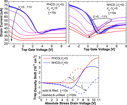
First we attempt to compare the degradation dynamics of pure PHCD and NHCD with different magnitudes. In
Figure 6.24(top) we show the transformation of the top gate transfer characteristics after subsequent pure PHCD and
NHCD stresses with increasing V d and ts=10s. Clearly, the impact of HC stress on the device performance depends on the
polarity of V d, which introduces some asymmetry between the two issues. PHCD shifts V D in an NBTI-like manner and
also leads to a deformation and vertical drift of the transfer characteristics. However, NHCD is of PBTI-like
nature at smaller V d and NBTI-like at larger V d while the transition at moderate V d is associated with a
current increase. The resulting ΔNT versus V d dependences (Figure 6.24(bottom)) allow us to conclude that
PHCD leads to the creation of positively charged defects, while NHCD introduces a negative charge at smaller
V d and a positive charge at larger V d. At the same time, an increase of ts makes PHCD more pronounced
while in the case of NHCD this leads to a stronger interplay between the defects of different signs. Another
interesting observation is that after the stresses with larger V d the magnitude of ΔNT tends to decrease.
This is most likely because of the disappearance of some positively charged defects, which also occurs in Si
technologies [69].
However, since under real operation conditions the hot carrier and bias stress components typically act in conjunction,
the analysis of the last four HCD issues mentioned in Figure 6.23 is of an even higher interest. Therefore, at the next
stage of our research we analyze PHCD and NHCD overlaid on either PBTI or NBTI with V tg-V D=±4V and
ts=1000s. While using our experimentral technique with constant ts and increasing V d, we also monitor the
recovery.
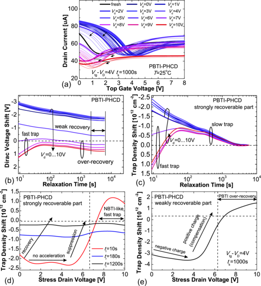
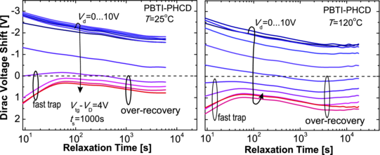
In Figure 6.25 the results for PBTI-PHCD are depicted. The degradation/recovery dynamics strongly correlate with the
magnitude of the applied HC stress. At smaller V d a PBTI-like shift of the Dirac point is observed which means that the
impact of bias stress dominates. However, at larger V d an NBTI-like PHCD first reduces the Dirac point shift and then
introduces an NBTI-like fast trap shift which is similar to pure NBTI in GFETs. The total ΔV D (Figure 6.25b) can be
separated into strongly recoverable and weakly recoverable parts; for convenience each is plotted in the units
of charged trap density shift ΔNT. The strongly recoverable part (Figure 6.25c,d) at smaller V d is mainly
associated with bias stress while at larger V d PHCD reduces it and also supplements an NBTI-like fast trap.
Interestingly, the slow trap behaviour remains PBTI-like and thus originates from the bias stress independently
of the HC stress magnitude. The weakly recoverable part (Figure 6.25e) at smaller V d originates from the
bias stress and reflects the presence of a negative charge which is then compensated by PHCD at larger V d.
Moreover, an extra positive charge appears after strong HC stresses which leads to over-recovery of PBTI-like
degradation.
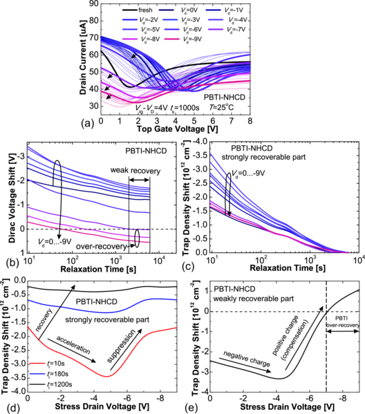
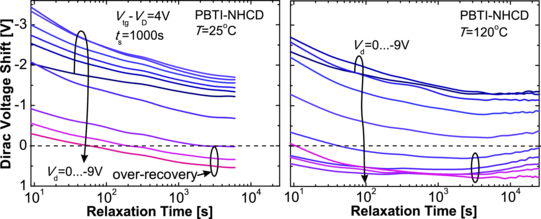
The related results for PBTI-NHCD are plotted in Figure 6.26. A PBTI-like nature of the NHCD component at smaller
V d results in a significant acceleration of the PBTI degradation while its NBTI-like nature at larger V d leads to its
suppression. However, contrary to the previous case, a more significant negative charge density prevents a complete
suppression of PBTI-like behavior. Thus, the strongly recoverable part remains PBTI-like within the whole V d
range and no NBTI-like fast trap appears (Figure 6.26c,d). The behavior of the weakly recoverable part
(Figure 6.26e) is similar to PBTI-PHCD, although an increase of negative charge density obviously proceeds faster.
Nevertheless, an extra positive charge leading to over-recovery of PBTI-like degradation is present at larger
V d.
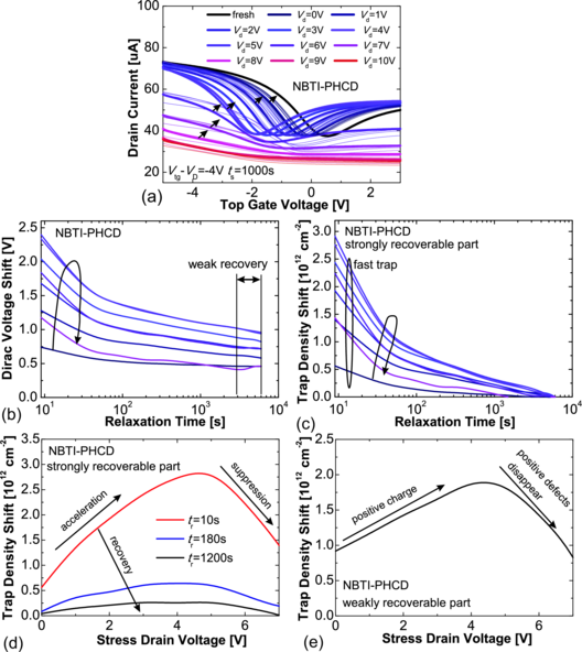
In Figure 6.27 one can see the results for NBTI-PHCD. Obviously, in this case both the HC and the bias component are
able to create only positively charged defects. Thus the degradation is NBTI-like within the whole V d range and no
over-recovery is observed (Figure 6.27b). However, a strong transformation of the shape of the characteristics (Figure 6.27a)
does not allow us to perform a reliable extraction of ΔV D for the largest V d. The strongly recoverable part
(Figure 6.27c,d) initially increases versus V d and shows the presence of an NBTI-like fast trap shift. However, the
stresses with larger V d lead to a decrease of the degradation which indicates that positively charged defects
disappear, similarly to Si technologies [69]. The weakly recoverable part (Figure 6.27e) behaves in the same
manner which suggests the absence of any interplay between the defects with different signs in the considered
case.
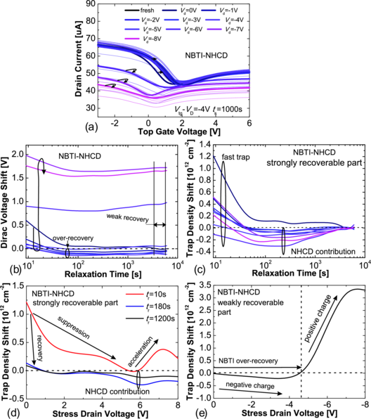
Figure 6.28 presents the related results for NBTI-NHCD. In this case the bias component is suppressed by the PBTI-like
NHCD component at smaller V d and becomes significantly pronounced at larger V d when NHCD is NBTI-like. Interestingly,
in all cases except V d=0 (pure NBTI) the strongly recoverable part (Figure 6.28c,d) in addition to the NBTI-like fast
trap contains a PBTI-like slow trap contribution which is obviously associated with NHCD. This means that
despite the overall NBTI-like nature at larger V d, NHCD creates some negatively charged defects. The weakly
recoverable part (Figure 6.28e) at smaller V d is associated with an insignificant amount of negative charges
which leads to over-recovery of NBTI-like degradation. At larger V d the positive charge results in incomplete
recovery.
The results above show that in the case of NBTI-PHCD we are dealing only with positively charged defects, while
NBTI-NHCD introduces a large amount of positive charges and some insignificant amounts of negatively charged defects. At
the same time, PBTI-PHCD and PBTI-NHCD are associated with a strong interaction between defects with opposite signs
introduced by the bias and hot carrier components. In order to study this interaction in more detail, we repeat our
experiments for the latter two issues at T=120oC.
In Figure 6.29 we compare the ΔV D recovery traces for PBTI-PHCD measured at T=25oC and T=120oC. Clearly, at
both temperatures we observe a strong suppression of PBTI degradation by the PHCD component and over-recovery as well
as an NBTI-like fast trap response supplemented at larger V d. However, comparison of the results obtained at different
temperatures shows that at T=120oC compensation of PBTI degradation by the PHCD contribution becomes pronounced
starting at smaller V d, while NBTI-like fast traps also appear earlier. Therefore, we conclude that the PHCD component is
accelerated at a higher temperature. The related results for PBTI-NHCD are shown in Figure 6.30. Contrary to the previous
case, the NHCD component is able to introduce some negative charges at smaller V d. This leads to acceleration of the
PBTI component at T=25oC. Conversely, a strong NHCD component acts in the same manner as PHCD and
leads to a compensation of the PBTI degradation and over-recovery. As for the case of T=120oC, the NHCD
component compensates PBTI independently of V d. However, NBTI-like fast traps are not present, which
suggests that some asymmetry between the PHCD and NHCD components is still pronounced at T=120oC.
Interestingly, for both PBTI-PHCD and PBTI-NHCD the weakly recoverable positive charges introduced by the
hot carrier components tend to recover at high T, i.e. the Dirac point starts to return back to its original
value.
6.7.3 Impact of HCD on Charged Trap Density and Carrier Mobility
The top gate transfer characteristics measured at different stress/recovery stages for various HCD issues in GFETs contain
the information on both charged trap density and carrier mobility. The former is associated with the Dirac point voltage
shift, while the latter can be captured by analyzing the shape of the Id-V tg curve at a certain recovery stage. Therefore, we
can now perform a more detailed analysis of the experimental results provided in Figures 6.25– 6.30, and study the
variation of the charged trap density and mobility after HCD stresses with different polarities. Also, a correlation between
the two quantities can be analyzed.
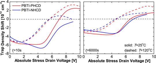
In Figure 6.31 we depict the resulting charged trap density shifts extracted from the recovery traces given in
Figures 6.29– 6.30. Clearly, the asymmetry between PBTI-PHCD and PBTI-NHCD observed 10s after the stresses
at T=25oC almost disappears at T=120oC (Figure 6.31(left)). The only conserved trend is that a strong
PHCD component introduces more positive charges than the NHCD component of the same magnitude,
while the difference is mainly due to NBTI-like fast traps. The related results obtained after 6000s recovery
(Figure 6.31(right)) show that both PHCD and NHCD components of large magnitude introduce weakly
recoverable positive charges. Obviously, the concentration of these defects is larger at a higher temperature, leading
to a stronger over-recovery (cf. Figures 6.29– 6.30). Also, the range of stress V d within which the charge
compensation takes place is wider at T=120oC. The reason for this is that not only the hot carrier, but also
the bias component becomes more pronounced at a higher temperature. Therefore, at T=120oC a strong
interplay between defects with opposite signs introduced by the PBTI and HCD components starts at smaller
V d.
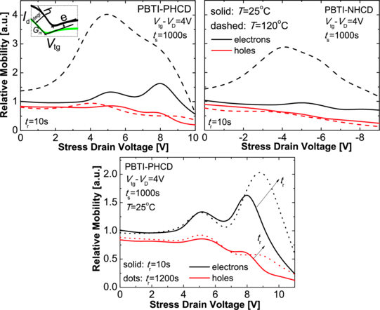
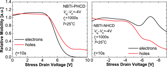
Analysis of the transfer characteristics given in Figures 6.25– 6.26 allows us to determine the transconductance Gm and
extract electron and hole mobility [178] at all PBTI-PHCD and PBTI-NHCD stress/recovery phases. In Figure 6.32, the
obtained values related to the mobilities measured before the stress (typically 20–60cm2/Vs for electrons and 90–150cm2/Vs
for holes) are plotted versus stress V d. One can see that in both cases the electron mobility increases with respect to its
initial value, an effect which becomes more pronounced at T=120oC. At both temperatures the electron mobility maximum
is located within the V d range corresponding to the charge compensation region (cf. Figure 6.31). This behaviour is more
likely related to screening effects [97] which accompany the interplay between the defects with opposite signs. Obviously, at
higher temperatures charge compensation starts at smaller V d but proceeds more slowly, making the interplay
between different defects and, consequently, the electron mobility maximum more pronounced. Moreover,
the relative decrease in electron mobility after the maximum is stronger than for holes. This is because of
the presence of additional positively charged defects. Such defects cause electrons and holes to experience
attractive scattering and repulsive scattering, respectively. Furthermore, attractive scattering is known to be
stronger than repulsive scattering [131]. Conversely, at small V d, when negatively charged defects dominate, the
relative degradation of the hole mobility is stronger. At the same time, in the case of PBTI-PHCD at T=25oC
there are two maxima: the first one corresponds to the beginning of charge compensation and the second one
appears near the transition point and significantly increases after the recovery of the fast trap component
(Figure 6.32(bottom)). The latter indicates that the positive charge introduced by the fast traps contributes to the
attractive scattering of electrons. Therefore, we can conclude that the observed mobility change not only
correlates with a variation of the charged trap density, but also agrees with the attractive/repulsive scattering
asymmetry reported in [131]. At the same time, the impact of screening effects on the mobility means that an
interaction between the defects with opposite signs introduced by bias and hot carrier components takes
place in terms of both their charges and potentials, while being considerably more pronounced at higher
temperatures.
In Figure 6.33 the related results for NBTI-PHCD and NBTI-NHCD measured at T=25oC (cf. Figures 6.27– 6.28) are
provided. In both cases the charge created at smaller V d is insufficient to cause significant mobility degradation because the
defects are mainly introduced by the bias component and therefore situated at a considerable distance from the graphene
channel. In the case of NBTI-PHCD, larger V d causes a nearly symmetric decrease of the electron and hole mobilities. This
suggests scattering at neutral imperfections [131, 97] which most likely substitute disappearing positive defects (cf.
Figure 6.27d,e). However, the degradation of electron mobility is stronger, which is due to the presence of positive charges.
Most likely, at larger V d these defects are situated in the proximity of the graphene channel, which makes their
contribution to attractive scattering of electrons more significant. The results for NBTI-NHCD show that
at moderate V d the electron mobility is affected by screening, similarly to PBTI-PHCD and PBTI-NHCD.
However, the magnitude of screening effects in the case of NBTI-NHCD is significantly smaller, since the
concentration of negatively charged defects is not enough for a considerable compensation of positive charges
(Figure 6.28).
6.7.4 Similarities to BTI and Fitting with General Models
The results for HCD discussed above were obtained using the V + sweep mode when measuring the top gate transfer
characteristics. That is why in the case of NBTI-like degradation, the presence of the fast trap response on the ΔV D(tr)
recovery traces is obvious. However, in the case of pure BTI, the suppression of the fast trap contribution using the V -
sweep mode allowed us to fit the experimental ΔV D recovery with the capture/emission time (CET) map model [69] and
the universal relaxation function [61, 64] previously developed for Si technologies. Taking into account the
similarities between BTI and HCD in GFETs, which are mostly associated with the absence of dangling bonds, we
proceed with applying these general models to fit the HCD dynamics in GFETs. In order to do so, we have
performed similar HCD experiments using our experimental technique which employs subsequent stress/recovery
rounds with constant V d and increasing ts, while using the V - sweep mode when measuring the transfer
characteristics.
As mentioned above, the CET map model [69] assumes that charge exchange associated with BTI degradation/recovery
is thermally activated, while the correlated activation energies can be described using bivariate Gaussian distributions. The
main parameters of the model are the mean values (μc and μe) and the standard deviations (σc and σe) of the capture and
emission energies Ec and Ee, respectively. In addition, an uncorrelated part of the emission energy ΔEe and the
corresponding μΔe and σΔe are considered. However, it was found that the use of the original model [69] not always produces
reasonable results, especially when trying to fit HCD recovery traces in GFETs. This is most likely because V D shifts in
GFETs are significantly larger than threshold voltage shifts in Si technologies. Therefore, we suggest modifying the
model [69] by changing the implict correlation between the standard deviations σe2=rσ
c2+σ
Δe2 with r being a new model
parameter which can be varied between 0 and 1, while in [69] r was equal to 1. Thus the distribution is given
by:
 | (6.21) |
The results obtained for NBTI-PHCD and PBTI-PHCD are shown in Figure 6.34. While only a single Gaussian
distribution corresponding to a more recoverable component has been used, the fits (Figure 6.34a,b) of the recovery traces
are rather reasonable. This underlines the similarity between HCD and BTI dynamics in GFETs. The underlying CET map
distributions (Figure 6.34c) are also similar to those obtained for BTI in GFETs (cf. Figures 6.13– 6.14). Moreover, the
dynamics of HCD in GFETs can be also described by the universal relaxation model [61, 64] (Figure 6.35). Remarkably, the
parameters B and β given in the plots are similar to their counterparts obtained from BTI data for both GFETs and Si
technologies (Figure 6.12). This further confirms the similarity in the physical mechanisms underlying degradation/recovery
dynamics.
However, the described analysis is typically only possible if both HC and bias components introduce defects of the same
sign (e.g. NBTI-PHCD). Otherwise, if the two contributions have opposite signs (e.g. PBTI-PHCD), fitting is only possible
for stress conditions under which the bias component dominates. At the same time, the dynamics of PBTI-PHCD with
comparable HC and bias components (e.g. Figure 6.29) are more complicated and therefore can not be described using such
simple models [61, 64, 69].
6.8 Chapter Conclusions
In summary, we have performed a detailed study of both BTI and HCD dynamics in GFETs. First, we found that
high-temperature baking of devices leads to a decrease in device-to-device variability, which either allows us to
perform numerous measurements on the same device or obtain consistent results for different stress conditions
on similar devices. Together with an optimized experimental technique, in which a constant oxide field is
sustained during all measurements, this allowed us to obtain experimental results for BTI in GFETs which
are fully consistent with Si technologies. Thus, the BTI assessment methodology suggested in this chapter
is generally suitable for quantifying the quality and reliability of graphene FETs and graphene/dielectric
interfaces. Furthermore, we have demonstrated that the BTI dynamics on the back gate of our GFETs are
similar to those on the high-k top gate, although the latter is less stable with respect to BTI. Next, we have
classified those reliability issues in GFETs which are associated with HCD and investigated their impact on
device performance. In particular, it was shown that the interplay between the bias and the hot carrier stress
components is stronger if the HC stress acts in conjuction with PBTI, while the qualitative drift-diffusion
simulations allowed us to understand the origin of this behaviour. Moreover, we have demonstrated that
HCD impacts both the charged trap density shift and the mobility which are correlated, while the mobility
variation agrees with the previously reported attractive/repulsive scattering asymmetry[131]. Finally, we have
demonstrated that, similarly to pure BTI in both GFETs and Si technologies, for some stress conditions the
long-term HCD data can be well fitted with the CET map model and also with the universal relaxation relation.
Therefore, our systematic method for benchmarking new graphene technologies was extended to the case of
HCD.