« PreviousUpNext »Contents
Previous: 1.3 Outline Top: Home Next: 2.2 Semiclassical Electron Dynamics
Investigating Hot-Carrier Effects using the Backward Monte Carlo Method
2 Semi-Classical Transport Theory
In quantum mechanics, electrons are treated as waves. For semiconductor devices with a slowly varying potential profile, however, carriers can be described classically as particles [65]. The interaction with the surroundings is modeled by scattering processes. The term semi-classical, in turn, stems from the conjoined classical electron dynamic and the quantum-mechanical treatment of scattering processes. The classical electron dynamic is derived from the band-structure of the material.
2.1 Band-Structure
Quantum-mechanics provides the basics to describe the possible states of carriers in a semiconductor lattice [60, 89]. The lattice is described with a periodic energy potential. The state of a carrier is described by its wave function, which is the solution of the Schrödinger Equation of the system [65].
![(2.1) \{begin}{align} i\hbar \frac {\partial \Psi }{\partial t} = - \frac {\hbar ^2}{2m_0}\nabla ^2 \Psi + \left [ E_{C0}(\vec {r}) + U_{C}(\vec {r}) + U_S(\vec {r},t)\right ] \Psi
(\vec {r},t). \label {eq:SE-T} \{end}{align}](main-images/image-46.svg)
The probability density of finding a electron in  is represented by
  . The potential energy in the equation above has three different parts [60]. The first part,
  , is the so-called built-in potential which results from the distribution of the ionized dopands in the semiconductor. The second part,
  , is the periodic crystal potential which results from the atoms’ electrostatic potential. And the third part,
  , is the scattering potential, which describes random potential fluctuations causing scattering processes. Further details about scattering mechanisms will be discussed later in this thesis.
Neglecting both built-in and scattering potential, Schrödinger’s Equation solely depends on the periodic crystal potential. Thus the time-independent Schrödinger Equation is given by [60]:

The wave-function in a periodic potential has the form of a Bloch wave [55, 77],

where  represents the crystal volume, and
  represents the crystal momentum. The Bloch functions are periodic,

where  is a vector of the direct lattice. When inserting the Bloch waves in the one-electron wave equation (2.2) with the periodicity condition (2.4), discrete eigenvalues

can be obtained [65]. Every eigenvalue is periodic in  -space.

where  is a vector of the reciprocal lattice. Each eigenvalue
  represents one band of the semiconductor. Because of its periodicity, all the information is included in one period which is called the Brillouin zone [65]. The band-structure of a one-dimensional lattice is shown in
Fig. 2.1.
represents one band of the semiconductor. Because of its periodicity, all the information is included in one period which is called the Brillouin zone [65]. The band-structure of a one-dimensional lattice is shown in
Fig. 2.1.

Figure 2.1: Band-structure of a one-dimensional lattice from the Kronig-Penny model [55]. The (first) Brillouin zone is indicated in red.
The electron-wave can propagate in three dimensions. Thus, the Brillouin zone is a volume [65]. The resulting geometric shape can be determined from the reciprocal lattice-vectors.
2.1.1 Reciprocal Lattice
The diamond structure of the silicon crystal comes with two atoms in its primitive cell. This kind of lattice can be represented as two intertwining face-centered-cubic (FCC) structures, see Fig. 2.2. Every point of the diamond lattice can be described with the following base-vectors [1, 36, 55, 96, 99, 111]:

Figure 2.2: Face-centered-cubic structure and its base-vectors

where  is the lattice constant of the crystal. The base-vectors (
 ) of the crystal lattice can be transformed in base-vectors (
 ) of the reciprocal lattice [54], which represent wave vectors [20, 96]:

The reciprocal lattice of the FCC lattice is face-centered cubic [110]. A Brillouin zone is defined as a Wigner-Seitz primitive cell in the reciprocal lattice [55]. The Brillouin zone of Silicon is an truncated octahedron [53, 67], shown in Fig 2.3.

Figure 2.3: Light gray: Brillouin zone of silicon; dark gray: the irreducible wedge
The band structure in this volume is highly symmetric and can be represented in just a fraction of the full volume and several symmetry operations. In the case of a cubic lattice, there are 48 symmetry operations [65]:
-
• 8 mirroring operations across a
 plane
plane
-
• 2 mirroring operations across a
 plane
plane
-
• and 3 rotation by
 along the
 ![\( [111] \)](main-images/58A5920CE4A00F1E795EFC2D70DC76C1.svg) direction.
direction.
These operations are illustrated in Fig 2.4.


This fraction of the Brillouin zone is called irreducible wedge and is defined by [65]

Fig. 2.3 showes the irreducible wedge and also the standard notation of the symmetry points in the Brillouin zone:
-
•
 represents the point
-
•
 represents the points at the BZ boundary in
  directions
-
•
 represents the points at the BZ boundary along the
  diagonals
At the symmetry points or along the axes between these symmetry points, there are often local minimum or maxima of the  relation, also called valleys. In simple band-structure models, every valley is approximated by a quadratic function as shown in Fig. 2.5.

Figure 2.5: Valley approximation of a band-structure. The -valley is in the point  . The X-valley is along the direction but not necessarily on the X-symmetry point. The L-valley is along the direction in the L-symmetry point.
2.1.2 Parabolic Band Approximation
Band-structures for commonly used semiconductors are known through experiments and numerical calculations [65]. The majority of electrons will stay at lower energies and will not reach most of the areas in the band-structure where energies are higher. Approximations are used to describe this majority of carriers around the energy minimum. For a given band-structure, a Taylor expansion can be performed [65].

The linear term is always zero for a minimum or a maximum. For semiconductors, where the energy minimum is at , the quadratic approximation can be written as

where

is the effective mass of one specific band-structure minimum [65]. This approximation shows that the electrons in a crystal can be treated like free electrons with different masses around the energy minimum.
The effective mass often display different values depending on the crystallographic orientation [65]. If a valley has rotational symmetry along one axis the effective mass can be split into one transversal and one longitudinal mass. In this case, (2.17) changes to
![(2.19) \{begin}{align} \Epsilon (\vec {k})=\Epsilon (\kv _0) + \frac {\hbar ^2}{2} \left [ \frac {\vec {k}^2_l}{m^*_l} + \frac {\vec {k}^2_t}{m^*_t} \right ]. \label
{eq:mass-tensor} \{end}{align}](main-images/image-96.svg)
This equation describes a band-structure with ellipsoidal constant energy surfaces in the main directions of silicon [102], shown in figure Fig. 2.6. Equation (2.19) uses a tensor for the effective mass and describes the conduction bands in the X-valleys and the L-valleys.

Figure 2.6: Ellipsoidal constant energy surfaces of the X-valleys.
The parabolic band approximation is derived for energies around the band minimum. At higher energies, other band structure models are required [46].
2.1.3 Non-Parabolic Band Approximation
For high applied fields, carriers may reach energies far above the minimum, and higher order terms in the Taylor series expansion (2.16) cannot be ignored. For the conduction band, non-parabolicity is often described by a relation of the form [21, 44, 65, 68]:

where  is the effective mass at the minimum and
  is non-parabolicity factor. For a direct semiconductor the non-parabolic factor of the -valley is given by [102]

with  being the energy gap.
2.1.4 Full-Band Structure
The non-parabolic band approximation can be used for energies up to  [65]. For carriers with higher kinetic energies, a more detailed description of the
  relation is needed. Models of physical processes such as impact ionization and carrier-carrier scattering, as well as reliability models are relying on an accurate description of high-energy carriers [P3]. A commonly used
method to handle carriers with higher energies is the full-band-structure [105], where the complete relation in the irreducible wedge of the Brillouin zone is provided [110]. The band-structure can be found by solving the Schrödinger Equation (2.1).
relation is needed. Models of physical processes such as impact ionization and carrier-carrier scattering, as well as reliability models are relying on an accurate description of high-energy carriers [P3]. A commonly used
method to handle carriers with higher energies is the full-band-structure [105], where the complete relation in the irreducible wedge of the Brillouin zone is provided [110]. The band-structure can be found by solving the Schrödinger Equation (2.1).
Empirical Pseudopotential Method
The empirical pseudopotential method is an effective way of calculating band structures of various materials. The method is derived from the orthogonal plane wave method [35] and the Phillips-Kleinman cancellation theorem [16,
17, 76, 96]. The key simplifications of this method is that the valence electrons determine the band-structure and the effect of the core electrons can be neglected [96]. The resulting potential, which is used in the Schrödinger
equation, is expanded into a Fourier series over the reciprocal lattice [105, 112]. The coefficients of this series are altered with form factors to fit the empirical data [56, 96]. One reason for the popularity of the empirical
pseudopotential method is the low number of parameters. Furthermore, the results yielded by this method are in many cases more accurate than ab-inito calculations [105]. Fig. 2.7 shows the band-structure in silicon, calculated by the empirical pseudopotential method [101].
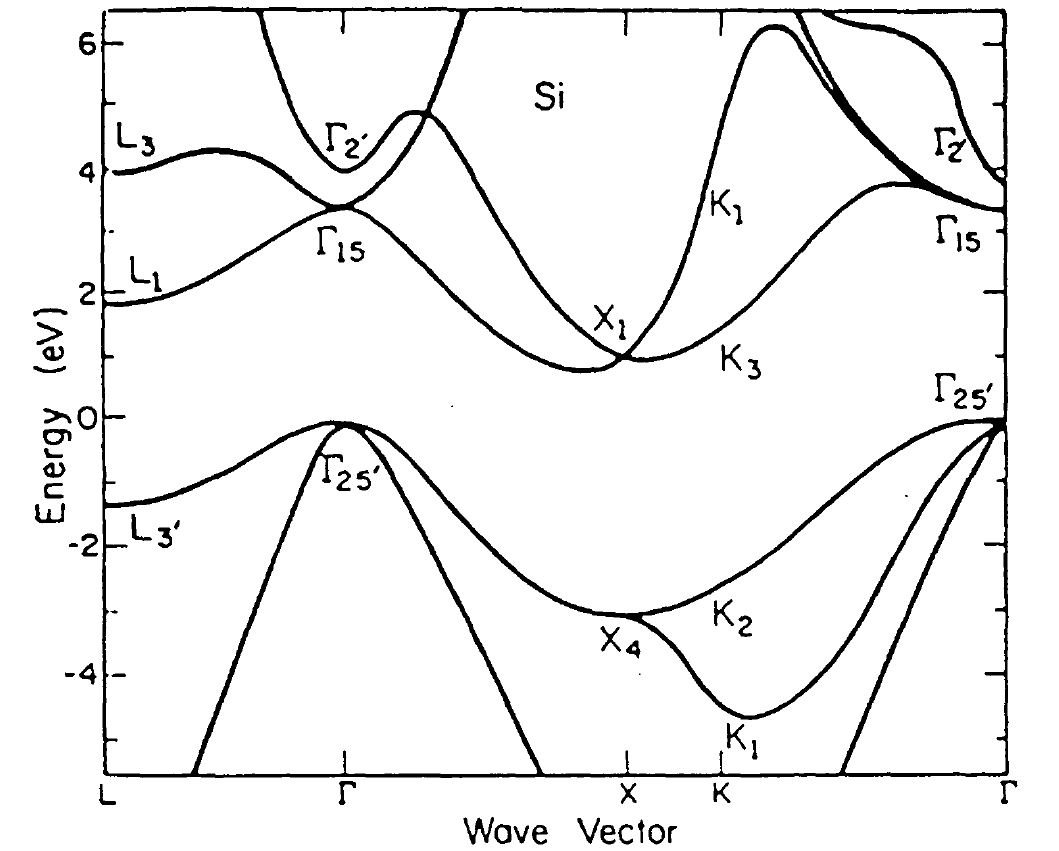
Figure 2.7: Silicon full-band-structure (picture taken from [60])
The three different band-structure approximations introduced above are compared for unstrained silicon in Fig 2.8, where the dispersion relation along the
![\( [100] \)](main-images/C2E4206CD3EA6AF572CE4F64BECC3B2D.svg) direction is illustrated. Moreover, it shows the need for a detailed description of the band structure above .
direction is illustrated. Moreover, it shows the need for a detailed description of the band structure above .

Figure 2.8: Comparison of the dispersion relation of unstrained silicon in direction of the axis with both parabolic and non-parabolic approximations, as well as EPM.
Previous: 1.3 Outline Top: Home Next: 2.2 Semiclassical Electron Dynamics