Finally, a nonlinear least-squares optimization is performed to determine the profile by adjusting the TPS coefficients in order to minimize the fit error between the simulated and measured capacitance data. Two types of capacitance measurements are taken on a fingered polysilicon structure over active area region. The source/diode region is surrounded by a gate on all sides to eliminate any capacitance coupling to the isolation area. Since the source/drain diode bottom area capacitance was matched while extracting the 1D source/drain profile, its value is subtracted from the total diode capacitance for both measured and simulated capacitance. This increases the sensitivity of the diode data to 2D profile variation in the lateral direction under the gate. Indeed, the main source of 2D channel doping information is the inner sidewall diode capacitance data.
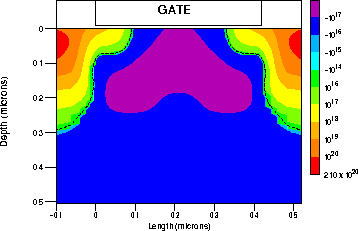
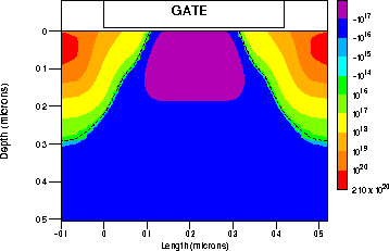
Figure 4.9: Extracted profile.
The capacitance measurements are taken under a variety of bias conditions that probe various portions of the doping profile by depleting or accumulating the carriers in that region. In view of the inherent interaction of the donor and acceptor doping via the net doping term in Poisson's equation, a coupled iterative scheme is used for solving the nonlinear least-squares problem. At each iteration, the coefficients of the acceptor and donor TPS are updated separately by taking one step in the Levenberg-Marquardt algorithm while keeping the coefficient of the other impurity type fixed. In addition, TPS coefficient at knots that are not of the same type as the net doping at that location are not included in the extraction.
The extracted profile is shown in Fig. 4.9. In Fig. 4.10 the experimental gate to source/drain capacitance are compared to the simulated values using the starting and extracted profiles. The fit improvement is apparent. Fig. 4.11 shows the corresponding inner sidewall diode data which also fit very well. By matching the experimental capacitance measurement the extracted profile is an accurate representation of the net dopant distribution in the device.
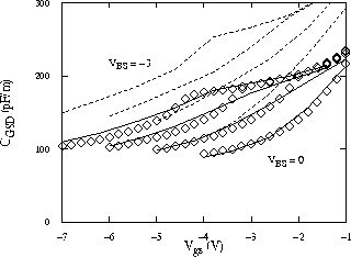
Figure 4.10: Comparison of experimental (symbols), simulation with starting
profile (dashed), and simulation with extracted profile (solid) gate to
source/drain capacitances  vs.
vs.  at varying
  .
.
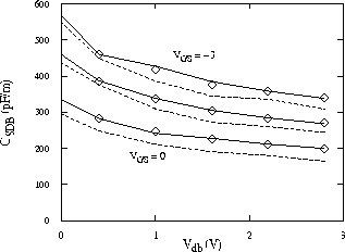
Figure 4.11: Comparison of experimental (symbols), simulation with starting
profile (dashed), and simulation with extracted profile (solid)
inner sidewall source/drain diode capacitances  vs.
vs.  at varying .
The method was also applied to three N-channel devices with varying implant
conditions as shown in Table 4.1.
Fig. 4.12 is a schematic diagram of half of an
N-channel MOSFET with the n- implant angle.
The implant conditions for devices A and B corresponds to
Large-Angle-Tilt-Implanted-Drain (LATID) implant
[40][39],
while device C received a regular Lightly-Doped Drain implant.
Fig. 4.13 compares the extracted net doping at the
SiO /Si interface for the three devices. It is clear that the 2D profiling
method is able to resolve the difference in the lateral diffusion length
as the implant angle/energy increases.
/Si interface for the three devices. It is clear that the 2D profiling
method is able to resolve the difference in the lateral diffusion length
as the implant angle/energy increases.
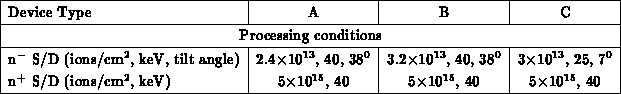
Table 4.1:
Processing conditions for Three N-channel MOSFET's
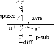
Figure 4.12: A schematic diagram of half an N-channel MOSFET with an
n- implant angle.
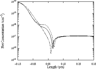
Figure 4.13: Extracted one-sided net doping at the SiO/Si
interface (device A - solid line, device B - dashed line,
device C - dotted line).