Previous: 2. Three-Dimensional Device Simulation Up: 2. Three-Dimensional Device Simulation Next: 2.2 Problems and Demands on Three-Dimensional Device Simulation
Three-dimensional device simulation is mandatory for investigations on real
three-dimensional structures because these structures cannot be described by
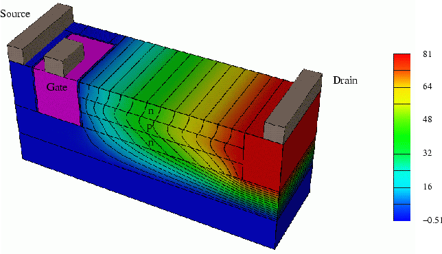
two-dimensional cuts. As an example, Fig. 2.1 shows the
three-dimensional structure of a Lateral Trench LDMOSFET. The figure shows the
device at breakdown with
![]() . The gate is built by a
trench whereas the channel forms at the sidewall of the trench gate vertically
in the device. Due to the super-junction concept the drift area is fully
depleted at breakdown. The potential is uniformly distributed to account for
the Reduced Surface Field (RESURF) effect.
. The gate is built by a
trench whereas the channel forms at the sidewall of the trench gate vertically
in the device. Due to the super-junction concept the drift area is fully
depleted at breakdown. The potential is uniformly distributed to account for
the Reduced Surface Field (RESURF) effect.
 |
Furthermore, three-dimensional simulations are mandatory when feature sizes become so small that the three-dimensional shape of geometries cannot be neglected. Thus two-dimensional simulations are no more reliable. A frequently cited example is the narrow channel effect of MOS transistors which are normally simulated in two-dimensional cuts. When the width of the channel becomes comparable to its length, the current path becomes clearly three-dimensional.
Another more obvious example is the temperature profile in real devices.
Two-dimensional simulations cannot predict temperature profiles very well,
because they do not take all cooling plates and directions of the heat flow
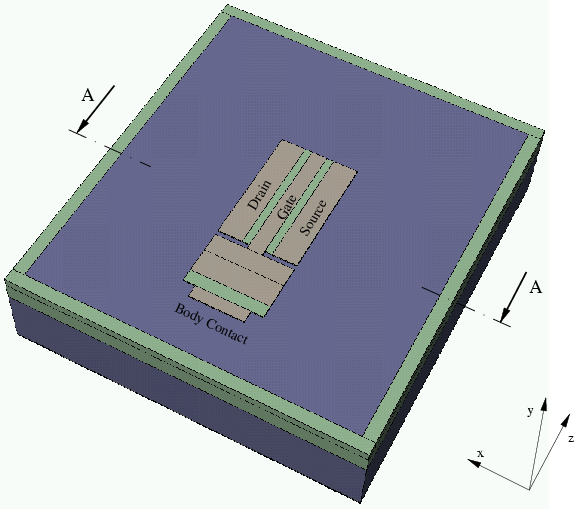
into account. As an example Fig. 2.2 shows the geometry
of a body contacted SOI MOS transistor. The gate is T-shaped and its length is
![]() and the width
and the width
![]() . The gate oxide thickness is
. The gate oxide thickness is
![]() . The transistor is surrounded by a rectangular silicon area of
. The transistor is surrounded by a rectangular silicon area of
![]() width which has been used here only to increase the cooling area and
therefore to make the resulting temperature profile more visible.
width which has been used here only to increase the cooling area and
therefore to make the resulting temperature profile more visible.
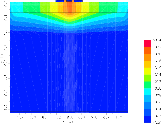
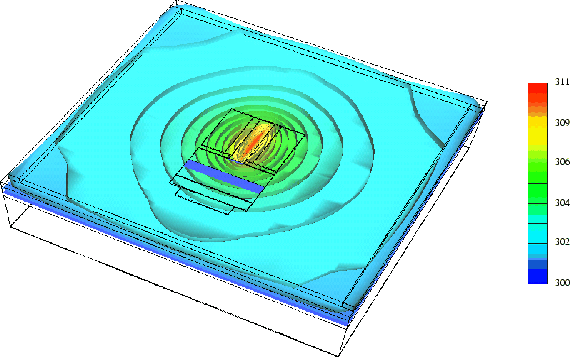
Fig. 2.3 shows the result of a three-dimensional
simulation. At the thermal contacts
![]() was applied. The
temperature profile is clearly three-dimensional contrary to the assumptions
made for two-dimensional simulations. At the end of the gate in
was applied. The
temperature profile is clearly three-dimensional contrary to the assumptions
made for two-dimensional simulations. At the end of the gate in ![]() -direction
the temperature is
-direction
the temperature is
![]() lower than in the middle.
lower than in the middle.
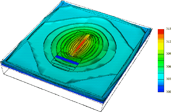 |
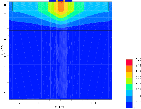
Fig. 2.4(a) shows the result of a two-dimensional simulation performed for the cut A-A depicted in Fig. 2.2. As a comparison, in Fig. 2.4(b) the same cut A-A is shown for the three-dimensional simulation of Fig. 2.3. As expected, the highest temperature appears in the channel below the gate and decreases with increasing lateral distance to the channel. Because the thermal resistance of SiO2 is much higher than that of silicon, a high temperature range is supplied by the gate.
|
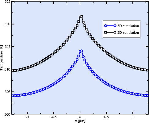
To clearly stress out this result the temperature at the surface of the silicon
segment of both the two-dimensional simulation
( Fig. 2.4(a))
and
the cut of the three-dimensional result
(Fig. 2.4(b))
is shown
in Fig. 2.5. It can be clearly seen, that the
two-dimensional simulation predicts a much higher temperature compared to the
three-dimensional one. The maximal temperature in the channel below the gate
is calculated as
![]() for the two-dimensional case and as
for the two-dimensional case and as
![]() for the three-dimensional case. Therefore, the error of
the temperature increase due to self heating made by the two-dimensional
simulation is about
for the three-dimensional case. Therefore, the error of
the temperature increase due to self heating made by the two-dimensional
simulation is about ![]() below the gate and about
below the gate and about ![]() at the side.
at the side.
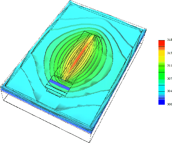
Fig. 2.6 and Fig. 2.7 show the
temperature profile of a body contacted SOI MOS transistor with a gate width of
![]() and
and
![]() , respectively. Both figures show a
three-dimensional shape of the temperature inside the device. But from these
figures one can clearly see the increasing importance of three-dimensional
simulations with decreasing feature sizes of the devices. Two-dimensional
simulations are no more accurate enough, not even for long devices.
, respectively. Both figures show a
three-dimensional shape of the temperature inside the device. But from these
figures one can clearly see the increasing importance of three-dimensional
simulations with decreasing feature sizes of the devices. Two-dimensional
simulations are no more accurate enough, not even for long devices.
 |
 |
Robert Klima 2003-02-06