Previous: 4.4 FinFET Up: 4.4 FinFET Next: 4.4.2 Simulation Results
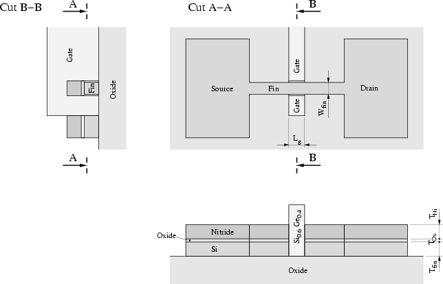
Fig. 4.21 shows the basic structure of a FinFET published in [163]. The device is formed on a thin silicon on insulator (SOI) finger termed fin. On the top of the silicon fin nitride has been deposited on a thin pad oxide to protect the silicon fin during gate poly-SiGe etching. The gates are formed at the vertical sides of the fin using a thin gate oxide layer. Gate work-function tailoring is essential to adjust the threshold voltage. Therefore, for the gate material poly-SiGe has been chosen. The crucial geometric device dimensions are:
The geometrical channel width is given by
![]() for one fin
since both channels have to be taken into account. To obtain higher drive
currents additional fins must be applied in parallel.
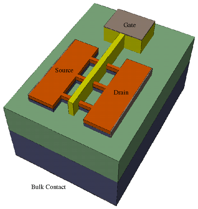
Fig. 4.22 shows a FinFET using three fins. Thus, with this
structure a three times higher drive current can be achieved.
The gate comb is formed as a small stripe which contacts the gates of all fins.
for one fin
since both channels have to be taken into account. To obtain higher drive
currents additional fins must be applied in parallel.
Fig. 4.22 shows a FinFET using three fins. Thus, with this
structure a three times higher drive current can be achieved.
The gate comb is formed as a small stripe which contacts the gates of all fins.
Robert Klima 2003-02-06