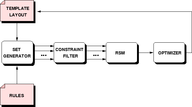
From these parameters, the geometrical dimensions play a chief role both in active and passive devices. For example, it is well known that the submicron devices are extremely sensitive to the channel length due to short channel effects [26]. The same applies to other devices (see the example of a laser trimmed resistor in Section 7.6) and obviously to lithography. Therefore, a method to automatically generate variatonal geometric information is needed. This demands for the generation of layout sets, parameterized according to rules to be specified. Thereby process engineers are assited in the tedious job of specifying geometric structures with different sizes.
The parameterized layouts can be linked with Response Surface Methodologies [27] to investigate the coupling between the layout and device/circuit performance in detail. This will also be advantageous in searching for critical dimensions and their optimization. The data-flow between these techniques is shown in Figure 3.5.
Typical applications are the determination of the optimal length and width of a transistor, the optimal width and pitch of interconnection wires, or the minimum distance between devices which is necessary to avoid substrate noise coupling.