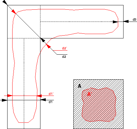
Besides checking the printability of a given layout, one should consider that real structures deviate from the layout also due to lithographic phenomena. Consequently, for a rigorous simulation of a given process step, it is not only necessary that the simulator itself is accurate, but also that the actual pattern transfered to the resist material used at that step is realistic. Typical examples of these lithographic effects occur in nested elbows of interconnect lines, where (with decreasing linewidth) the corners get bloated and the elbows rounded (cf. Figure 3.13 and Figure 3.14). Nevertheless, three-dimensional simulation of all steps related to pattern transfer is too complex and time/resources consuming and a simplified method to simulate large layouts is necessary.
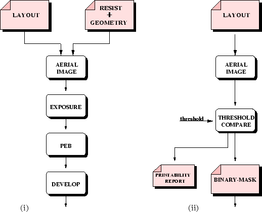
A typical lithography simulation flow includes an imaging module where the aerial image (the light intensity incident on the top of the wafer) is calculated. To achieve this, the light propagation through the optical system and the light transmission through the photomask is simulated. Next, there is the exposure module which simulates the chemical reaction of the photosensitive resist material. This requires that the light propagation in the resist and electromagnetic scattering effects are modeled. Finally, in the development module, an isotropic etching process, whose etching rates were calculated in the previous module, is simulated. Sometimes bake steps are also considered. This sequence is illustrated in Figure 3.11-(i).
From the described modules, the exposure tool has extremely long
run times. The simulator described in [33] needs, for a small
![]() mask, several hours which makes it impracticable even
for layouts with only few transistors. In the proposed approach, only
the aerial intensity image (with relative fast run time for medium size
layouts) is calculated. Afterwards, it is compared at each point with a
threshold value in order to generate a binary aerial image that is
used as a conventional binary mask in the further process simulation
steps - see Figure 3.11-(ii). As in this process contours
with very sharp and small edges can be produced, they are smoothed using
digital image techniques. An
advantage of this method is that phase shift masks are converted into
normal binary masks and do not need any special processing.
mask, several hours which makes it impracticable even
for layouts with only few transistors. In the proposed approach, only
the aerial intensity image (with relative fast run time for medium size
layouts) is calculated. Afterwards, it is compared at each point with a
threshold value in order to generate a binary aerial image that is
used as a conventional binary mask in the further process simulation
steps - see Figure 3.11-(ii). As in this process contours
with very sharp and small edges can be produced, they are smoothed using
digital image techniques. An
advantage of this method is that phase shift masks are converted into
normal binary masks and do not need any special processing.
In this approach the missing simulation steps are replaced by the threshold, and a careful choice of this value is critical. In our solution, it can be entered manually by the user or calculated automatically. In the latter case we extended the method presented in [32] where a complete two-dimensional simulation (as in Figure 3.11-(i)) is performed and the threshold value adjusted to obtain the best match with the simulation results. We follow the same idea, but using three-dimensional simulation. This allows us to find the best match considering corners and other critical features that do not have any axis of symmetry, as well.
To compute the aerial intensity image on the resist surface,
the simulator illum2d [34] which is integrated
in PED, is used. After performing these tasks it is possible to
generate a report of printability of the input layout, where the
critical nets (if existing) are pointed out. This is obtained by
comparing the original layout with the resulting binary aerial
image. Our algorithm follows the center lines of the patterns
in the resulting layout (exactly at the same coordinates of the
original) and checks if the width (at the perpendicular direction) in
that path is kept between some limits in relation to the equivalent in
the original layout (in Figure 3.12 if
![]() and
and ![]() ). At the corners the width is calculated from
the inner point to the exterior boundary in angular
increments (
). At the corners the width is calculated from
the inner point to the exterior boundary in angular
increments (![]() and
and ![]() in the same figure). The shrinking at line
ends (
in the same figure). The shrinking at line
ends (![]() )
is also compared against a maximum allowed value. In small
features, as contact holes, the checks are based on the area reduction
factor
)
is also compared against a maximum allowed value. In small
features, as contact holes, the checks are based on the area reduction
factor ![]() (see also Figure 3.12).
(see also Figure 3.12).