Traditionally, as already stated in Section 1.1, the design
and fabrication phases of VLSI integrated circuits are uncorrelated and
circuit designers have only to obey the layout rules. These are, however, a
compromise found for a given process when considering parameters as
performance, reliability and yield. The layout design rules are usually
conservative and sometimes not the best choice for a particular
design. This is becoming worse in
deep-submicron technologies as
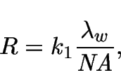
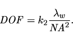
imaging systems are improving resolution-![]() not only by decreasing
the exposure wave length -
not only by decreasing
the exposure wave length - ![]() , but continuously increasing the
lenses Numerical Aperture66#2 (NA), which in turn
reduces the depth of focus (DOF) as given by the Rayleigh
scaling equations:
, but continuously increasing the
lenses Numerical Aperture66#2 (NA), which in turn
reduces the depth of focus (DOF) as given by the Rayleigh
scaling equations:
Yet, reducing the DOF causes severe restrictions to the maximum roughness allowed in the wafer surfaces [29], which is becoming a formidable problem, as planarization techniques are expensive and not extensively available. Some improvements in DOF and resolution are obtained using phase-shift masks that are supported by our layout editor.