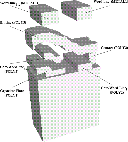
We studied a variation of the stacked trench cell [86] already presented in Section 6.2.3. Please, recall the care taken in the fabrication of the trench and in the dielectric formation. The study was divided into two parts: Initially only the storage capacitor was carefully simulated, and the interconnection lines were considered planar as it was presented in Figure 6.14. Then we performed a topography simulation for the complete cell, including the interconnect lines the solid model of which is given in Figure 7.5.
The experimental data and the extracted capacitances for both cases are presented in Table 7.1. From these results we conclude that simple models strongly underestimate the parasitic capacitances. For the bit-line the accuracy was improved by a factor of 5, confirming the need for topography simulation prior the capacitance extraction.
The small
difference still existing in relation to the measured value is due to the
disregard of the capacitance between adjacent bit-lines and due to
variations in process parameters. The value of
![]() in
Table 7.1 is for the case of 128 cells sharing the
same bit-line. The number of simulation nodes was
in
Table 7.1 is for the case of 128 cells sharing the
same bit-line. The number of simulation nodes was ![]() and
and ![]() for
the first and second
cases, respectively, corresponding to run times of 10 and 21 minutes on a
DEC 3000/400 workstation, obeying an almost linear dependence.
for
the first and second
cases, respectively, corresponding to run times of 10 and 21 minutes on a
DEC 3000/400 workstation, obeying an almost linear dependence.
| Planar | Non-planar | Measured | |
| fF | fF | fF | |
| 40.1 | 40.1 | 38.2 | |
| 1.04 | 1.72 | 1.88 | |
| 2.22 | 3.35 | - | |
|
|
0.34 | 0.42 | - |
|
|
3.3 | 5.5 | 6.3 |