next up previous
Next: 7.2.1 Trench Capacitor DRAM Up: 7. Applications Previous: 7.1 Ring Oscillator Revisited


7.2 DRAMs

The DRAM is the flagship product of the semiconductor industry. Obtaining a sufficiently large value of storage capacitance in a reduced cell area is becoming harder and harder and causing a more complicated capacitance electrode. Even using dielectric films with higher permittivity the capacitor structures are highly non-planar and their capacitances can be calculated rigorously only with numerical simulation techniques.

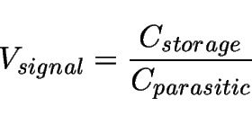
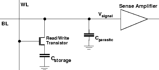
In a DRAM the information is stored as charge in a capacitor. In the reading process, the output signal amplitude is given (see Figure 7.4) by:


\begin{displaymath}
\vspace{0.1cm}
V_{signal}= \frac{C_{storage}}{C_{parasitic}}
\vspace{0.25cm}
\end{displaymath} (7.1)

Figure 7.4: Simplified DRAM schematic.
\begin{figure}
\vspace{0.25cm}
\centerline{\epsfig{file=APPdramFunc.eps,width=0.80\linewidth}}
\vspace{0.25cm}\end{figure}

A minimum storage node capacitance is necessary to make the ratio (7.1) sufficiently high to provide enough signal for the sense amplifier and to meet the retention time specifications. Hence, a focal point in the development of new DRAM cells is the optimization of the storage capacitor while keeping the parasitic capacitances as low as possible [85].

DRAM cells developed over the years from the simple planar capacitor to the families of trench capacitor and stacked capacitor cells which today, by far, dominate over all the other possible configurations. Although driving very different process technologies, our tools are suitable for simulation of both families, as the following examples demonstrate.


next up previous
Next: 7.2.1 Trench Capacitor DRAM Up: 7. Applications Previous: 7.1 Ring Oscillator Revisited
Rui Martins
1999-02-24