


Next: 4.3 Package Modeling Interface
Up: 4. Integration between Semiconductor
Previous: 4.1 Introduction
Subsections
The different interfaces identified can be seen in
Figure 4.1. The shaded areas in Figure 4.1
indicate the different interfaces between ``reality'' and ``simulation''.
Figure 4.1:
Scheme of identified interfaces between TCAD and
semiconductor fabrication
|
According to the work flow outlined in Chapter 3, the layout of the masks is one of the
two main inputs for process simulation.
Normally this layout is available in GDSII-binary format which can be read by
any of the above mentioned commercially available TCAD tools.
To mirror the activities carried out in the mask shop this data must undergo
the same transformations as in reality listed in Subject 4 of
Section 2.1. The ``Mask Generation Instructions''
define special boolean operations to modify the mask data in a way that
certain effects of wafer processing are cancelled out. Examples for possible
corrections like simple mask biasing or proximity corrections are given in
Section 3.3.2. An example for typical ``Mask Generation
Instructions'' is given in Table 4.1. The mask levels
are defined by the GDSII mask numbers given in the layout data file. The mask
description identifies every generated reticle by name and is the reference for the
lithography step in fabrication. The working plate field gives the data type
for each mask. ``DK'' means dark field and ``LT'' means light
field. The type gives an indication if the layout data has to be inverted
for mask generation. Light field masks are masks which are generated as defined by the GDSII data. Dark field masks are generated with
the inverted GDSII data. The contact mask is an example for a dark
field mask. Since the contact mask has to be used for etching a hole (which is
later filled with metal) into the oxide layer covering the silicon wafer, the
photoresist covers all areas which are NOT contact. Therefore the
GDSII data showing the contacts in the layout has to be inverted before mask
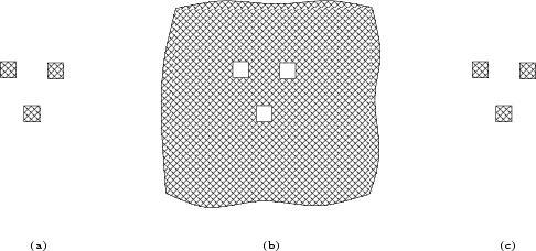
generation. Figure 4.2 shows this situation.
Figure 4.2:
Example for a contact
layer GDSII mask layer information (which is of dark field type) (a),
the corresponding chrome mask recticle and resist shape (neglecting proximity correction) (b) and the resulting etched
contact holes in the oxide layer (c)
 |
The biasing colummn give the bias to be applied to the GDSII data to
get the final chrome mask dimensions. The strongest bias has to be applied to
the mask level 10 listed in Table 4.1 which
compensates for the effect shown in Figure 3.4 in
Section 3.3.2. Since modern lithography steppers use 5x projection, the
structures on the recticle are five times bigger than they are projected onto the
photoresist. For mask quality control the critical dimensions of the chrome
masks are defined in the ``reticle CD'' column in Table 4.1.
Table 4.1:
Example of mask generation instruction table including biasing and CD
(critical dimension) information
| RESIST TYPE: POSITIVE |
| Mask |
Mask Description |
Working |
Biasing |
5x |
| Level |
|
Plate |
 /side /side |
Reticle |
| |
|
Field |
(1x) |
CD () |
| 5 |
n-Well Mask |
DK |
0 |
3 |
| 8 |
p-Well Mask |
LT |
0 |
|
| 10 |
Active Area Mask |
LT |
+0.08 |
2.4 |
| 8 |
p-Well Mask |
LT |
0 |
|
| 24 |
VTP-Implant Mask |
DK |
0 |
|
| 48 |
Anti Punch Through Mask |
DK |
0 |
|
| 14 |
Gate Oxide |
LT |
0 |
|
| 20 |
Poly 1 Mask |
LT |
+0.02 |
2 |
| 29 |
High Resistive Mask |
LT |
0 |
|
| 30 |
Poly 2 Mask |
LT |
-0.04 |
3.0 |
| 21 |
n-LDD Mask |
DK |
0 |
|
| 24 |
p-LDD Mask |
DK |
0 |
|
| 23 |
N+ S/D Mask |
DK |
0 |
|
| 24 |
P+ S/D Mask |
DK |
0 |
|
| 34 |
Contact Mask |
DK |
+0.02 |
2.2 |
| 35 |
Metal1 Mask |
LT |
0 |
2.5 |
| 36 |
Via 1 Mask |
DK |
0 |
2.5 |
| 37 |
Metal 2 Mask |
LT |
0 |
3 |
| 38 |
Via 2 Mask |
DK |
0 |
2.5 |
| 39 |
Metal 3 Mask |
LT |
0 |
3 |
| 41 |
Via 3 Mask |
DK |
0 |
2.5 |
| 42 |
Top Metal Mask |
LT |
0 |
3 |
| 40 |
Pad Mask |
DK |
0 |
|
|
Figure 4.3 shows the detailed structure of the identified
interface as motivated by the real mask generation and lithography
process. The GDSII data is converted into the ASCII formatted CIF format (for
easier processing) This data is then subject to boolean and biasing operations
as defined by the mask generation instructions. To emulate the real shape of
the photoresist a proximity correction is applied and the resulting contours
are written back to a CIF format serving as mask information input during the
process simulation.
Figure 4.3:
Interface of layout-data to simulation mask-data
|
A detailed description of the algorithm is given in Chapter 5.
4.2.2 Between Process Flow Description and Process Simulation Command File
The overall process flow information is typically documented in the database
of a manufacturing execution system like PROMIS [149] from
Brooks-PRI, SiView [150] from IBM, or
WorkStream [151] from AppliedMaterials.
The information relevant for process simulation inside this database is numerous,
depending on the detailed level of the simulation models (as outlined in
Table 3.1). Normally the following datasets are
needed for process simulation:
- Sequence of process steps representing the semiconductor process flow
(oxidation
 layer thickness measurement
implantation
diffusion
material deposition
lithography etc.)
layer thickness measurement
implantation
diffusion
material deposition
lithography etc.)
- Blocks of process sequences which are carried out on the same
semiconductor fabrication equipment and are normally organized as program
sequences like oxidation/diffusion programs which can consist of up to
dozens of single process steps with different temperatures (temperature
ramps) and gas ambients (gas steps or ramps).
- The detailed process parameter set of one single process step (e.g. ion
species and composition, ion dose and energy, angle of incidence and
rotational orientation of ion beam with respect to wafer, ion beam
divergence, etc., for ion implantation)
- Positions in the full semiconductor process flow where selected physical
characteristics like layer thickness or sheet resistances are measured by
using metrology tools on wafer level.
Subject 1 through
Subject 3 represent the hierarchy levels from highest
to lowest. It is advisable to use an abstract representation of data as an
intermediate format between the process step information and the simulation
command file. Since commercial simulators and simulators from university are
still under heavy development, syntax changes of the simulator command files
are happening frequently. Therefore a direct translator between process flow
information and simulation is inflexible and difficult to extend. With an
intermediate abstract format different types of simulators can be supported by
a single source of data (see Figure 4.4).
Figure 4.4:
Interface of process flow information to process simulation
command files
|
Typically the Manufacturing Execution System (MES) is not storing the full details of the diffusion and
oxidation recipes, the plasma etch programs or the etch and deposition rates
of the wet chemistry used during semiconductor processing. This information is
stored in separate databases as outlined in Figure 4.4. Normally
there is only a reference to a machine recipe or a etch sink given in the MES
flow. Again the strategy of exactly mirroring the real situation was chosen to
set up the interfaces. The recipes are transferred by a converter
into the meta-syntax and are then converted into the simulator syntax of the
process simulator chosen. This procedure is shown on the left hand side of
Figure 4.4. The converted recipes are then transferred into a
subroutine format, provided by every commercial or university simulator
available. Thus this approach can be used for every TCAD environment
available. Furthermore, through the use of a meta-syntax the interpretation of
the data formats inside the manufacturing system (MES and recipe databases)
and the conversion into the different simulator syntaxes can be treated in a
more systematic way, since both tasks cannot interfere in a single program but
are performed in a modular way. Last but not least the meta-syntax enables a very
compact and concise overview about the details of the semiconductor process
flow. Thus, this syntax can be used as a source for a very sophisticated
process flow description for documentation and training (see Section 6.2).
The details of the implementation and examples for the meta-syntax used are
given in Chapter 5.
After finished processing of the silicon wafers the first electrical test is
the measurement of simple test structures and devices organized in Process
Control Monitors (PCM) in the scribe-lines of the wafer. These measurements
are carried out on automated tester systems on wafer level. The measurement
procedures are again hierarchically oriented in the following way:
- Measurement program set up for actual technology node.
- Subprogram defined for actual PCM (normally several PCMs are inserted
in the scribe-lines).
- Module for Device Under Test (DUT) consisting of single program
statements measuring relevant electrical parameters.
- Single measurement algorithms for e.g. CMOS threshold voltage, or
diffusion sheet-resistance.
- Single steps of carrying out the measurement algorithm for e.g. CMOS
threshold voltage in saturation. These steps define how the device terminals
are connected to the voltage and current sources of the automated tester and
how the currents and voltages of the DUT are measured.
Subject 3 to Subject 5 are
mirrored on the device simulation side to provide comparable electrical data
of measurements and simulation.
Since the algorithms under Subject 4 and
Subject 5 are not changing frequently (the algorithms under
Subject 5 are fixed4.1 with the
hardware of the automated tester used and measurement algorithms defined under
Subject 4 are only changing, if a completely new
device type is introduced) these algorithms are not converted on a daily
basis. The structure of the interface is shown in Figure 4.5.
The subprogram conversion of the DUT modules is carried out much more frequently on a
daily basis.
Figure 4.5:
Interface of electrical wafer acceptance test information to
device simulation command files
|
There are two main application areas existing for converting electrical test
programs. First, this conversion is used for the automated generation of big
device test-chips during process development including new device
architectures. Second, the standard PCM structure measurement algorithms have
to be converted to match the simulation results with the PCM
measurements. Both methods are described in Chapter 5 in detail.
4.2.4 Between Device Characterization and Device Modeling (SPICE)
This interface deals with the generation of reliable device models for circuit
modeling (e.g. SPICE). The main devices (NMOS/PMOS transistors for standard
CMOS processes and, in addition, bipolar transistors for BiCMOS processes) of any
new process fabrication must be characterized completely in terms of output
characteristics, transfer characteristics, amplification, etc. This task
results in scalable electrical models (BSIM3 for CMOS, VBIC for Bipolar
transistors) or compact models for circuit simulation.
In the TCAD fabrication integration scheme the source for this fitting
procedure can be twofold: First, the usual way of measuring the
characteristics on semiconductor wafer material and second, by simulating these
characteristics with device simulation.
The second approach has the enormous advantage of getting worst case
predictions [152], [153], which are directly related to
process parameter changes by applying statistical variations on selected
semiconductor process step parameters (e.g. selected implantation doses).
Furthermore, combined process and device simulations without the existence of
any semiconductor material can generate preliminary models very early in the
process development stage.
Unfortunately the generation of SPICE models (e.g. BSIM3.3 or BSIM4 with
hundreds of free parameters) is not an
automated straightforward task. The process characterization engineers have to
set up many initial values for starting the optimization of actual
SPICE models and have to follow a complicated iterative strategy to get a good
model with reasonable accuracy. Therefore an automated global optimizer for
generating a good SPICE model is not available. Currently the only way to get
so called ``TCAD based models'' is to generate characteristics with device
simulation as they were measured on a real device and submit this information
to process characterization engineers for the generation of SPICE
models. Nevertheless, this approach enables the generation of a design
environment of a new technology in a very early stage of a process
development. The time to market for new process technologies is thus significantly reduced.
Footnotes
- ... fixed4.1
- these algorithms are typically
provided by the tester vendor in the form of test libraries
Next: 4.3 Package Modeling Interface
Up: 4. Integration between Semiconductor
Previous: 4.1 Introduction
R. Minixhofer: Integrating Technology Simulation
into the Semiconductor Manufacturing Environment
![\includegraphics[origin=c,width=1.40\textwidth,clip=true]{figures/wat_interface.rot.ps}](img184.png)
![\includegraphics[origin=c,height=2.1\textwidth,clip=true]{figures/overall_interfaces.2.ps}](img180.png)
![\includegraphics[angle=0,origin=c,height=0.5\textheight,clip=true]{figures/layout_interface.ps}](img182.png)
![\includegraphics[angle=0,origin=c,width=1.4\textwidth,clip=true]{figures/process_interface.ps}](img183.png)